This thread has been locked.

If you have a related question, please click the "Ask a related question" button in the top right corner. The newly created question will be automatically linked to this question.

TCAN4550: TCAN4550 Vccout pin gives 5.5V output

Part Number: TCAN4550

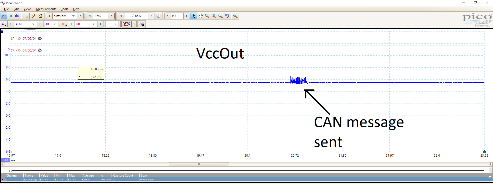
The VCCout  pin gives 5.5V when supplied with 15V supply.

SPI communcation is working fine.

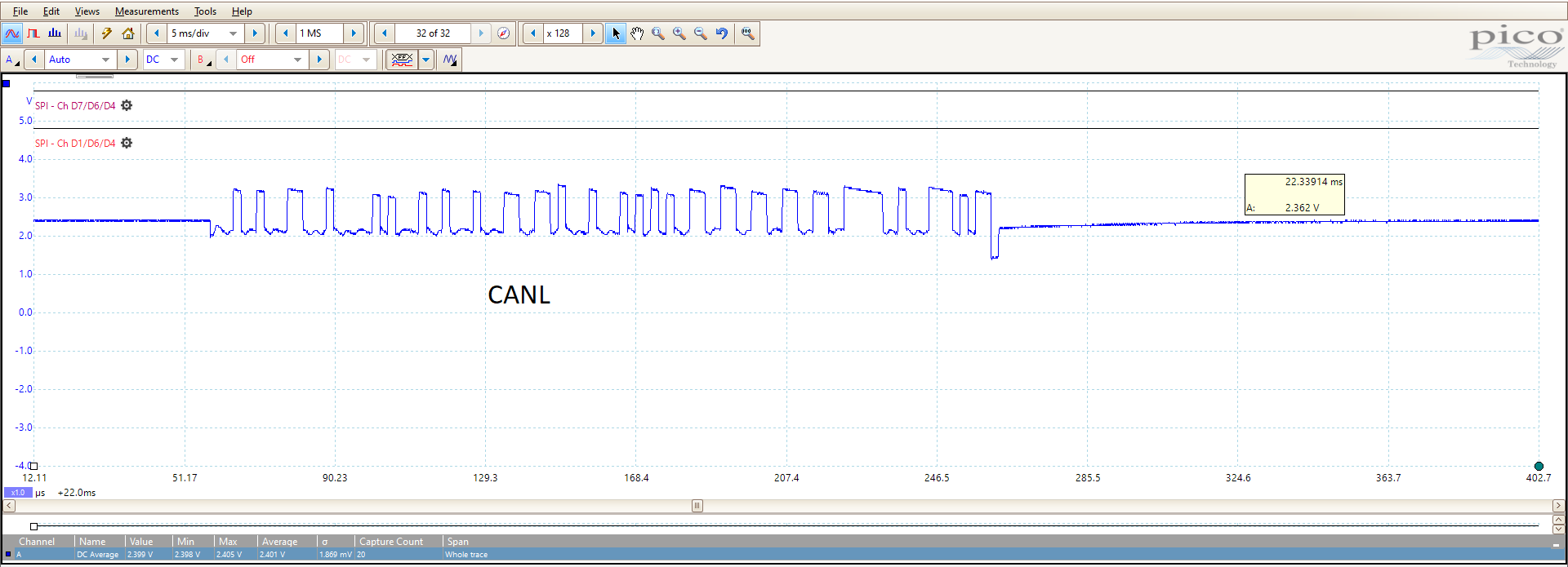
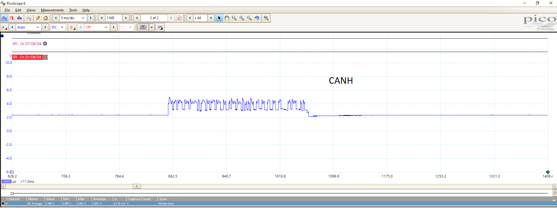
The 0.5V offset in VCCout also appears in CAN bus while message is being sent. The CANH and CANL pins remain near 2.5V and as soon as transmit messages command is sent a 0.5V offset gets introduced and refence voltage becomes 3V while sending CAN message. After transmitting message it returns back to 2.5V. Due to this some CAN messages sent by TCAN4550 are not received by receiver.

Also TCAN is not able to receive some CAN messages.

I have made schematics according to TCAN4550 EVM

  • Uday,

    Are you able to share your board schematic & any scope shots if available?

    The thread has been assigned to a App's engineer & he will help follow-up.

    Thx!

  • Hi Uday,

    I have just tested the EVM with a 15V supply and I did not see the same behavior you have described.  I see the VCCOUT voltage stay constant at 5V and the CAN bus VCM stay constant at 2.5V for the recessive level.  I have also verified that communication is good with other nodes on a simple bus that are powered off of 12V.

    I suspect there may be something in the schematic that is causing this problem.  If you can share those on this forum that would be great.  But if you would prefer to share them privately, let me know and I will send you a direct email to you at the email address linked to your E2E account.

    Regards,

    Jonathan

  • [TCAN1.PrjPcb] TCAN1.PDF

    Thanks Ravi and Jonathan

    This is my schematics

  • Below I have attached scope shots of CANL, CANH and VCCout while CAN message is sent by TCAN

    Thank you

  • Hi Uday,

    Thank you for providing the schematics and waveforms.  They are very helpful.

    Section 8.3 of the datasheet discusses the requirements and behaviors for all of the pins.  This is a good source for determining if all of the requirements have been met.  After reviewing your schematic, I have the following observations and recommendations:

    1. The Vsup pin requires a 100 nF capacitor at the pin and you have a 100 pF.  I would recommend changing C9 to a 100 nF value.
    2. The Vio pin requires a 100 nF capacitor at the pin and you have a 100 pF.  I would recommend changing C3 to a 100 nF value.
    3. The Vccout pin requires a 10 uF external capacitance and you have 0.33 uF.  I would recommend changing C2 to a 10 uF value.
    4. The nINT and GPO2 pins are an open drain architecture and requires an external Pullup Resistor.  I do not see them in the schematic but they may be located on the device you are connecting to these pins through the header.  If they are not included in the other board/device, then you will need to add the pullup resistors to these nets for them to work properly.  However, if you are using the TCAN4550 in one of the test modes, then these pins do not require a pullup resistor. (This is an observation unrelated to your current issue).

    My initial thoughts on the route cause of this behavior is specifically the less than required decoupling capacitance on the VCCOUT pin but generally for all the supply pins (Vsup and Vio) as well.  Please increase those values based on the datasheet values I've recommended and see if it makes any improvement.  I'll try to explain my thoughts.

    The TCAN4550 has an internal LDO that will regulate the Vsup voltage to a 5V voltage.  This 5V voltage is used to power the internal digital core, the CAN FD Controller, and provides the bias voltage for the CAN transceiver and is the source for the 2.5V recessive voltage level on the CAN bus (VCC/2).  The Vio supply powers the level shifting bias circuitry on the digital IO signals and also powers the OSC/CLKIN circuitry, but the digital core primarily operates from the 5V rail.  If the voltage changes too much, it could also create errors inside the digital core and could be the reason messages are not received properly.

    This 5V LDO is capable of providing more current than is required by the TCAN4550 and therefor it can be used to power external circuitry such as a MCU through the VCCOUT pin.   As you have observed, any variation to the LDO's output voltage will directly affect the CAN bus voltage.  Variations in the current load requirements will need to be tracked and accounted for by the LDO and the external capacitance connected to the LDO is a critical component of this circuit.  As I have pointed out, the datasheet states a 10 uF capacitance is required on the VCCOUT pin to maintain output voltage stability. 

    When the capacitance is too small, the current load change resulting from a CAN message happens much faster than the LDO feedback loop can track and therefore the voltage level changes as the LDO tries to compensate.  When the capacitance is large enough, the extra current can be sourced through the stored charge in the capacitor and allow the LDO enough time to compensate without causing a change in the voltage level.  The scope capture of the VCCOUT voltage clearly shows that simple activity such as transmitting a CAN message can cause a large voltage deviation which I believe points to the 0.33 uF capacitance added to the VCCOUT pin being too small.

    If you are still having issues after adjusting the cap values, please let me know.  However, I hope that this change will make a noticeable improvement.

    Regards,

    Jonathan

  • Thank you Jonathan

    I will test and reply in few days.

  • I checked by increasing capacitance values, now CAN is working properly without errors. However, I am still getting 5.5V at Vccout.

    Thank you

    Regards

    Uday Mumbaikar

  • Hi Uday,

    I'm glad to hear the additional capacitance has stabilized the CAN communication.  However, the 5.5V output voltage is definitely on the high side and greater than the 5.2V maximum specification.  I did not see anything in the schematic that would justify this excess voltage.  Do you have more than one of these boards with the TCAN4550?  If so, do they too measure 5.5V?  I am wondering if this device has been damaged.  If you only have one board, have you tried a different TCAN4550 device on that board?

    Regards,

    Jonathan