This thread has been locked.

If you have a related question, please click the "Ask a related question" button in the top right corner. The newly created question will be automatically linked to this question.

TLIN2021-Q1: TLIN2021-Q1

Part Number: TLIN2021-Q1

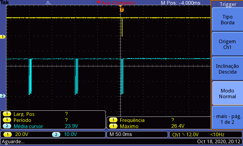
The master LIN controller manages to put the tanceiver in sleep mode after putting EN to zero. AND INH goes HZ as expected. BUt when connected to slave LIN, it does not work, INH still putting +24V no diabling the DCDC converter. There is no LIN activiity on the bus wich is in recessive mode. Why connecting to a SLAVE LIN would prevent master to go sleep mode if there is no LIN activitty.

  • There appears to be a similar post regarding this same issue. I'll consolidate both posts to this thread and remove the previous one. 

    RP:
    "We are implementing a LIN design deploying TLIN2021 as a master LIN. When LIN controller forces ENABLE to low level and the INH pin goes High Impedance as it supposed to work, putting the DCDC converter off and the microcontroller its self turns off entering sleep mode, But when the master is connected to a slave, it does not work, even putting EN to 0V, INH still VLIN . !There is no LIN activity whatsoever in the bus, we connect a oscilloscope and the bus is in recessive state.

    What might explain such a behaviour?"

  • Hi Ricardo,

    When the EN pin is Low, TLIN2021 will either be in Sleep Mode (with INH disabled as high-z) or in Standby Mode (where INH is driven to Vsup). The device will transition from Sleep to Standby when it detects a wake up condition on the LIN bus, or when the WAKE pin is triggered. You can also identify when the device is in Standby Mode by observing the RXD output as low regardless of the state of the bus.

    It is possible that connecting the Primary LIN node to the bus causes it to recognize false WAKE conditions and in turn cause the transition from Sleep to Standby Mode. During your tests, do you observe the INH signal to drop after EN is driven Low? Or is there no activity on the INH signal when this is done? Also, are you able to observe the state of the bus at the time that EN is driven low? Any scope shots you can share showing the voltage levels and relative timings would be helpful to identify the cause of this behavior.

    Would it also be possible to share a schematic of this design? I'm primarily interested in how/if INH is pulled down, what connections are made to the WAKE pin, and any other bias resistors to determine default pin states.

    Let me know if you believe there's any other information that may help with this debug.

    Regards,
    Eric Schott

  •  Hello Eric , I will provide some scope shots soon. Meanwhile sharing with you part of the schematic, I can't share all fo it because this design is protected by NDA, I work as a consultant for the company who owns the design. I am implementing the software only althought I reviwed the hardwre and looks good to me. 

    I will send now only the scope I have right now  ....looking at output of the converter(yellow) and EN_LIN( blue). Works fine....if the master is not connected to the slave LIN..

    thank you Eric

  • Hello Eric , I will provide some scope shots soon. Meanwhile sharing with you part of the schematic, I can't share all fo it because this design is protected by NDA, I work as a consultant for the company who owns the design. I am implementing the software only althought I reviwed the hardwre and looks good to me. 

  •  I work with Ricardo in this design...

    CH1 (Yellow) - PIN EN

    CH2 (Blue) - PIN IHN with 100k pull down add.

    CH1 (Yellow) - IHN PIN;

    CH2 (Blue) - LIN PIN;

    CH1 (Yellow) - EN PIN;

    CH2 (Blue) - RXD PIN

  • Eric, after taking a look at osciloscope pictures, we relizaed there was a LIN activity while EN was forced down. Problem solved, thank you

    Ricardo

  • Hi Ricardo, Duan,

    Glad to hear you were able to identify the cause of this behavior. Thanks again for sharing.

    Regards,
    Eric Schott