Part Number: TCA9535
Other Parts Discussed in Thread: IO-EXPANDER-EVM
Hi team,
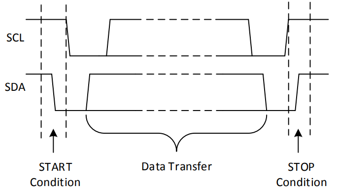
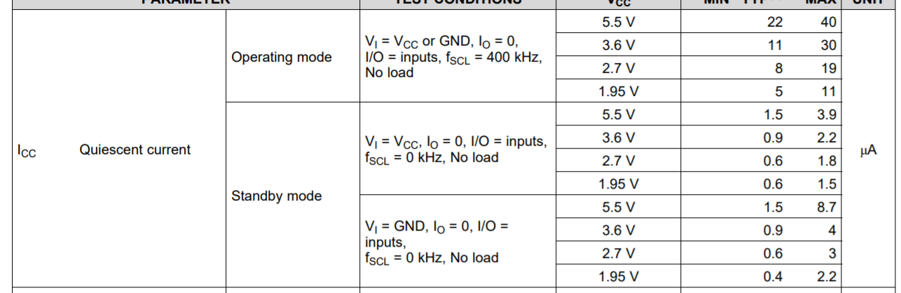
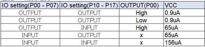
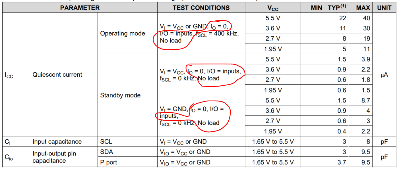
Could you tell me how to set the standby mode?
Only set SCLK=0kHz?
Sincerely.
Kengo.
Part Number: TCA9535
Other Parts Discussed in Thread: IO-EXPANDER-EVM
Hi team,
Could you tell me how to set the standby mode?
Only set SCLK=0kHz?
Sincerely.
Kengo.