Part Number: SN65DPHY440SS
Tool/software: Code Composer Studio
Dear TI Support team
When I use dphy440 as a repeater, I encounter the following problems: using 4lane mode (single lane mode is also tested, the phenomenon is consistent)
1,My test platform is normal. My PCB design is designed in strict accordance with the signal characteristic specification, and the corresponding impedance matching has been done. To ensure that the test platform has no problem, I first connect senro to my platform, test OK, and then connect it to dphy440 board. (one module for sensor, one module for dphy440 and one module for master control).
2, The sensor of Sony imx214 series can output signal and plot normally after adding dphy440. The input and output of signal measured by oscilloscope are normal;
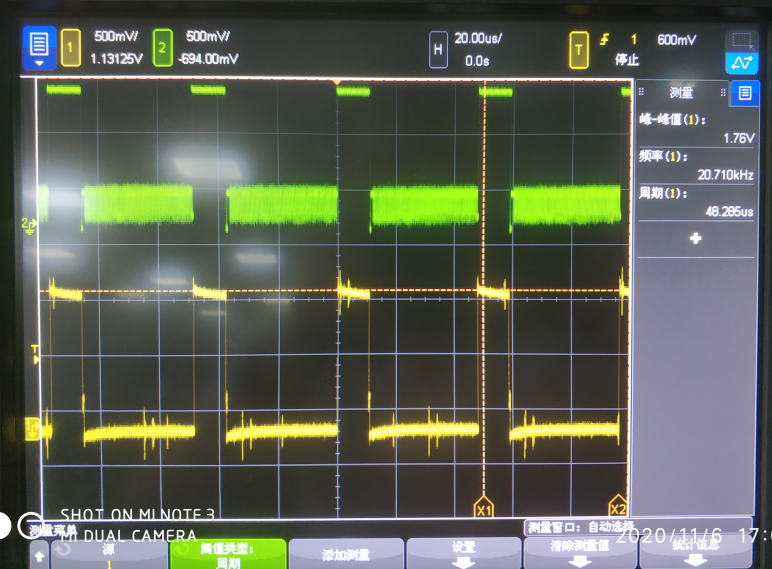
3, The sensor of Sony imx314 series can not output the image. After measuring with oscilloscope, it is found that the four pairs of differential pair signals output from the sensor end to the input end of dphy440 chip are normal; however, the lane0 from dphy440 output end to main control chip has no HS signal, and the other three Lane signals are normal. Reduce the speed to very low (6mhz) phenomenon is the same;
4, I put cfg0, cfg1, erc, EQ have combined debugging, the problem is still the same.
5, After I cut off the dphy440 board to the main control chip, I found that the DB end of dphy440 has HS signal output;
6, Try some other sensors, some normal, some abnormal, abnormal phenomenon, such as Sony imx314.