This thread has been locked.

If you have a related question, please click the "Ask a related question" button in the top right corner. The newly created question will be automatically linked to this question.

DS160PR410: Cannot detect devices

Part Number: DS160PR410


Hi Team,

My customer design DR160PR410 for PCIe[x4] application and found "device no detect" issue. The failure rate is 10pcb/60pcs, engineer found it might related to SMT process issue since he re-mount devices again on 4 FA boards then can fix these boards. He will try it on the other FA boards to see if all of them have same problem.

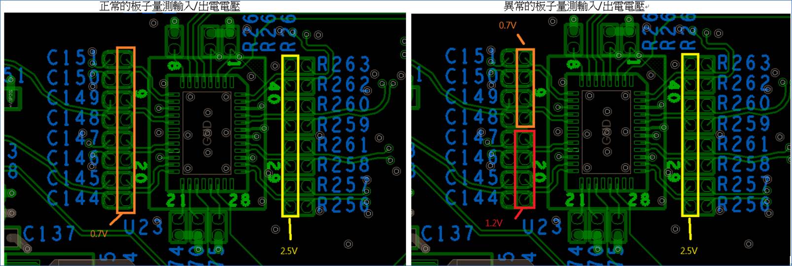
Engineer did some measurement on FA and good boards and the result as following.

Here is partial SCH. 

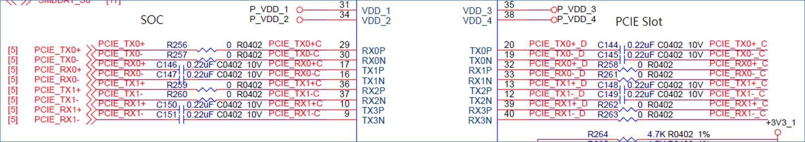
The left picture shows the good PCB's result, the signal level of TX side is about 0.7V.

The right picture shows the FA PCB's result, red frame shows abnormal signal level of 1.2V.


1. Customer would like to know what kind of SMT failure can cause this failure phenomenon?

2. After PCB SMT process, can customer measure TX or RX pins' signal level to determine it's a good or FA board without transmitting real signals?

If the description above is not clear or further information is needed, please let me know.

Thanks very much.

Vincent Chen 

  • Hi Vincent,

    Given after re-mounting the part, the failure board worked, it is suggested to do the followings:

    1). Use ohmmeter to measure impedance between pins both for a non working board and a good board. We can use this result to problematic pin.

    2). If possible, on a non-working board and instead of remounting, try to re-heat or resolder one pin at a time to see if this takes care of the problem. This can tell us if cold solder could be causing this issue.

    3). On a non-working board, is it possible to heat up the thermal pad under the device just to make sure there is good connection between thermal pad and copper under the device? Please compare pcb layout to make sure solder paste mask and vias meet data sheet recommendation(note date sheet figure 14 and note regarding recommended foot print layout).

    Regards,, Nasser

  • Hi Nasser,

    Thanks very much for the advices. 

    My I know what is the impedance range between TX/RX versus ground?

    In this part there is no ground pin except thermal ground pad, I am thinking what if thermal pad is not soldered well then how can I detect it? Is there ESD protection diode on pins? Please could you comment it?

    I have provided your suggestions to customer and ask them to provide PCB layout for reviewing.

    Thanks a lot.

    Vincent Chen

  • Hi Vincent,

    1). We should see about 100 ohm on high speed TX or RX when RX termination is detected. Please note you may see high impedance if there is no termination on the output of the device.

    2). Through x-ray we can detect if thermal pad is well connected or not. Also, comparing and checking different pin voltages between working unit versus non-working unit can help as well.

    3). There ESD protection diodes on every pin.

    I am not sure if reviewing the pcb layout may help here. I think there could be a manufacturing process such as solder profile that could be playing a role here. You may want to check solder profile on this package and make sure we are following this requirement during manufacturing of the board.

    Regards,, Nasser

  • Hi Nasser,

    I really appreciate your comments and I will forward them to customer and talk to R&D. I will let you know if we need any further support.

    Thanks a lot.

    Vincent Chen

  • Hi Nasser,

    Some information updated from customer.

    2). Through x-ray we can detect if thermal pad is well connected or not. Also, comparing and checking different pin voltages between working unit versus non-working unit can help as well.

    --> Customer make 200pcs boards and there are 140pcs un-test. Customer will start testing rest boards, if they found same issue they will use x-ray to compare fail and good pcs to see is there any clues.

    3). There ESD protection diodes on every pin.

    --> Customer did P-N junction measurement and function verification were PASS.

    Below is customer's PCB layout. 2 units per board, dark blue is pad, green is solder mask. I don't see anything improper.

    Except above, I got one information that when customer tested single board they fix them to gen1 and gen2 and all PCBs can pass test. Once the boards were assembled into system which will set to auto detection then few pcbs were failed. Do you have any ideal for such kind of phenomenon?

    Thanks very much.

    Vincent Chen

  • Hi Vincent,

    Regarding your question, i think this could still be a manufacturing or a pcb related issue.

    Through TI internal email, you can send me pcb layout in .brd format (Cadence pcb layout ) and i can review this layout in more details.

    Regards,, Nasser