This thread has been locked.

If you have a related question, please click the "Ask a related question" button in the top right corner. The newly created question will be automatically linked to this question.

DS250DF230EVM: Loop back mode, need to get CDR lock

Part Number: DS250DF230EVM
Other Parts Discussed in Thread: DS250DF230, DS250DF210,

I have the board setup to try to get the loop back mode working, but I am not able to get CDR lock.  I am supplying 3.3V to the board.

  1. On the p5 of the EVM User's Guide, it shows that I need to install J41 and leave J45 open.  I just want to confirm that's a misprint.  I have J41 open and installed jumpers to J45 so there's 2.5V to the chip.
  2. I have to MXP40 connectors connected to the board, and have the signals go from TX0P --> RX0P, TX0N --> RX0N, etc... for all the signals.
  3. The best that I could ever get was "Signal Detected" on Channel 1 (but not on Channel 0), and I am not able to get CDR Lock.
  4. Can you let me know what I need to do to get CDR Lock?
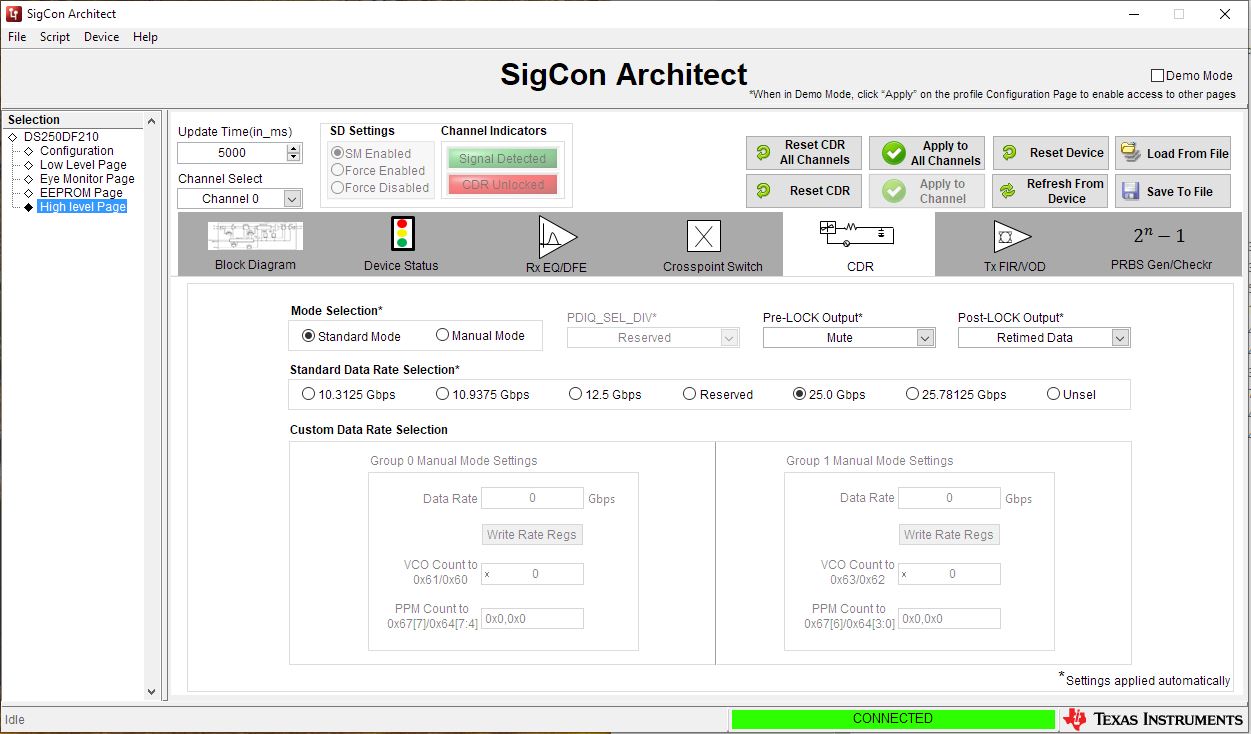
    On the CDR Tab I have: Pre-LOCK Output: Pattern Generator, Post-Lock Output: Retimed Data, Data Rate: 10.3125 Gbps
    PRBS Gen/Checker: Enable, PRBS31.

Thank you very much for your help!

Jack Lin

  • I also noticed that when I enable the PRBS Generator, I am not able to run the PRBS Checker.  Is this true?  We were hoping to run the PRBS generator on the TX side and PRBS check on the RX side at the same time to check the BER in loopback.  Is this possible?

  • I guess I should try to explain what I am trying to do:

    1. With the MXP40 connectors, we are looping back the signal from TX to RX.
    2. We want to output PRBS patterns on the TX, and check it on the RX.
    3. We want to try the Eye Diagram functions.
    4. We want to try to run it at different data rates.

    I tried to check the TX outputs on the scope, and they either look flat, or some random noise.  They do not look like PRBS patterns.

    Is there a .cfg file that we can load up for the default? Or do we need to run a sequence of commands to get it going?

    I also noticed that if I go to Script -> Launch Window, the program would crash and I get this error message:

    Error 5000 occurred at Notifier Timed Out
    Re-Driver Device GUI.lvlibp:GUI Wait for GUI Response via Notifier.vi:1:\Re-Driver Device GUI.lvlibp:Launch Macro Recording.vi\Re-Driver.lvlib:Main.vi

    This error code is undefined. Undefined errors might occur for a number of reasons. For example, no one has provided a description for the code, or you might have wired a number that is not an error code to the error code input.

    Additionally, undefined error codes might occur because the error relates to a third-party object, such as the operating system or ActiveX. For these third-party errors, you might be able to obtain a description of the error by searching the Web for the error code (5000) or for its hexadecimal representation (0x00001388).

  • Hi Jack,

    1). Please follow EVM user guide directions. J45 should not have any jumper and install J41. Then apply 2.5V to J44 and GND J42 (nothing connected on J43). Also, please use EVM schematic for further guidance.

    2). Please follow link below for generating and checking PRBS:

    https://e2e.ti.com/support/interface/f/138/t/701759?tisearch=e2e-sitesearch&keymatch=%252525252520user%25252525253A90220

    Regards,, Nasser

  • Thank you Nasser.

    1. On the EVM User guide, it says to connect 3.3V to the board (p5), hence my confusion.
    2. On my eval board, there is only 1 DS250DF230 installed ("1", left side).
      Is it possible to have the TX of 1 chip looped back to the RX of the same chip?

      From your link, it seems to suggest that we will need 2 chips, 1 for sending out the PRBS, and 1 for checking the PRBS?

    Thank you again for your help!
    Jack

  • Sorry, some more questions for our eval board:

    1. If RX0 is open, can TX0 still output PRBS?  Or we HAVE to provide a clock signal to RX0 for TX0 to work?
    2. Since we only have 1 chip on our eval board, if we provide clock to RX0, and connect TX0 to RX1.  Will we be able to send out PRBS on TX0 and check the PRBS on RX1?

  • Greetings,

    1). Yes we have to provide a clock or a data pattern and get the first device to lock. Once it is locked, you can enable PRBS generator.

    2). Yes you can do as you noted.

    Regards,, Nasser

  • Hi Nasser,

    What's the lowest freq we can supply to RX0 for it to lock?

    Do we need to configure the CDR of Channel 0 to match the clock freq for it to lock?

    Thank you,
    Jack

  • Hi Nasser,

    I am following the steps from the PRBS pattern post:

    1. Power on the board and connect to the software.  The board is drawing 0.09A from 2.5V.
    2. Supply the 3.125GHz clock to RX0.  The power draw goes to 0.19A. (The scope capture was done with a diff probe on C52, C54, the AC caps for RX0)
    3. On the software, I see that it has "Signal Detected".
    4. I changed the Data Rate to 25G on the CDR Tab.
    5. I am not able to get CDR lock.

    Am I missing any steps?  What should we do to get the board going?

    Thank you,
    Jack

  • Also, I want to confirm.  On the eval board user guild, it says on the device selection I need to select DS250DF230.

    But on my SigCon, it shows DS250DF210.  I want to make sure that is not a problem and not a source of our trouble.

    Just FYI, we also tried to hook up the output of a different chip that generates PRBS31 at 12.5G, 6.25G, & 3.125G to the RX0 of the chip.  We get signal detected, but also no CDR lock.

    Is it possible that our eval board is defective?  How can we confirm?

    Thank you,
    Jack

  • Hi Jack,

    1). First please note clock has to be integer multiple of your data rate. 3.125GHz clock frequency that you are using should be fine. 

    2). Secondly, looking at your clock waveform, we should have close to 50% duty cycle - meaning close to d0% high and close to 50% low. Also, please make sure you use differential clock.

    3). After making changes to the GUI, please make sure you click on Apply to All Channel.

    4). Please note earlier link that i sent and follow these steps. These are the steps we did in our lab and other users have been able to do the same as well.

    Regards,, Nasser

  • Hi Nasser,

    1. The clock we are suppling is a differential clock.
    2. As an experiment, we also try supplying PRBS31 patterns at 3.125G to RX0.
    3. We followed the steps closely several times, and we also repeated it to supply the clock to RX1.  Same results.
    4. We made sure that we clocked on "Apply to All Channel".

    Can you let us know what are the possible reasons CDR is not locking?  Is it possible that we have a defective chip?

    Thank you,
    Jack

  • Hi Jack,

    I just went to lab and used 3.125GHz clock source and am able to get the device to lock. Please note image below. I am thinking there could be issue either with your clock source or perhaps there is something wrong with the part. Normally these devices and EVM get tested before getting shipped. You may want to use different clock source and as long as it is integer multiple of the 25GHz it should enable the device to lock at 25Gbps.

    Regards,,, Nasser

  • Hi Nasser,

    Thank you for checking for us.

    We double checked our clock source to make sure it's ok:

    It's 3.125 GHz and 200 mV swing.

    I also made sure that I followed all the steps carefully.

    At this point we have to say we might have a defective board?
    Do you know how we should proceed to get a replacement?

    Thank you,
    Jack

  • Hi Jack,

    Please confirm that your are correctly setting the retimer channel for 25Gbps CDR rate, via either channel register 0x2F (i.e. Standard Mode) or channel registers 0x60 thru 0x63 (i.e. Manual Mode).

    A couple additional things to try.

    • Try increasing your 3.125GHz reference signal amplitude to say 400mVpp
    • Try disabling the retimer PPM check by setting channel register 0x2F[2]=0

    Cordially,

    Rodrigo Natal

    HSSC Applications Engineer

  • Hi Rodrigo,

    After I set it up, R2F = 0x44, R60 ~ R63 = 0x00.

    I tried setting R2F[2] = 0, which is R2F = 0x40, and I still couldn't get CDR lock.

    With our setup, we are unable to change the amplitude of the 3.125GHz.

    Is there anything else I should try?

    Thank you,
    Jack

  • Hi,

    What CAL_CLK_IN frequency jumper setting are you using on your EVM, 25MHz or 30.72MHz?

    Cordially,

    Rodrigo

  • Hi Rodrigo,

    It's the default of 30.72MHz. (I didn't change anything from the default, and it's 30.72MHz).

    Thanks,
    Jack

  • Hi,

    For the DS250DF230 the channel registers 0x60 thru 0x63 settings below should be used to configure CDR rate when 30.72 CAL_CLK_IN is used. Note the values for 25Gbps.

    Table. Register Settings for Common Data Rates using 30.72-MHz Calibration Clock (DS250DF230 Only)

    DATA RATE

    REG_0x60 VALUE [HEX]

    REG_0x61 VALUE [HEX]

    REG_0x62 VALUE [HEX]

    REG_0x63 VALUE [HEX]

    REG_0x18[6:4] VALUE [HEX]

    25.78125 Gbps (1)

    74

    B4

    74

    B4

    0

    25.0 Gbps

    DD

    B2

    DD

    B2

    0

    24.33024 Gbps (1)

    80

    B1

    80

    B1

    0

    20.625 Gbps

    F6

    A9

    F6

    A9

    0

    20.0 Gbps

    B1

    A8

    B1

    A8

    0

    12.5 Gbps

    DD

    B2

    DD

    B2

    1

    12.16512 Gbps (1)

    80

    B1

    80

    B1

    1

    10.3125 Gbps (1)

    F6

    A9

    F6

    A9

    1

    10.1376 Gbps (1)

    40

    A9

    40

    A9

    1

    9.8304 Gbps (1)

    00

    A8

    00

    A8

    1

    Cordially,

    Rodrigo Natal

  • Hi Rodrigo,

    I've tried your suggestions, but still unable to get CDR lock.

    R018 = 0x00

    Regards,
    Jack

  • Hi Jack,

    Could you click on "Save config" on the TI GUI low-level page to save your full register configuration file for when the issue is observed? And then share it with me?

    Thanks,

    Rodrigo

  • Hi Rodirgo,

    I am attaching 2 files.  1 with the Standard 25G setup (done on the CDR tab), the other using manual register writing to R60~R63 and R18.

    Thank you,
    JackStandard_Setup_25G.cfgManual_Setup_25G.cfg

  • Hi Rodirgo,

    Just wondering if you had a chance to take a look at our .cfg files.  Do you think we have a defective board?  If we do, how do we go about getting a replacement?

    Thank you,
    Jack

  • Hi Jack,

    • What is the data rate and pattern being used for the input signal to the DS250DF230 retimer?
    • What CAL_CLK_IN frequency are you using?

    Cordially,

    Rodrigo Natal

    HSSC Applications Engineer

  • Hi Rodrigo,

    • I am supplying a 3.125GHz clock as input.
    • The CAL_CLK_IN is 30.72 MHz

    We are using the DS250DF230EVM eval board, and we are following the suggested steps to get it running.

    Thank you,
    Jack

  • Hi Jack, we have duplicate threads. Let's close this thread and work from the other thread please. In the future try not to send duplicate messages on the E2E forum.

    Thanks,

    Rodrigo

  • Sorry, I thought we are still on the same thread/topic.

    Please let me know where to continue.

    Thank you,
    Jack

  • Hi Jack,

    Please make sure that the retimer settings for channel registers 0x60 thru 0x64 are correct for your data rate and CAL_CLK_IN. See table below. beyond that you may try the following:

    • Forcing CTLE = 0x00 - see routine below

    Table. Set CTLE Boost Value


    STEP

    SHARED/ CHANNEL REGISTER SET

    OPERATION

    REGISTER ADDRESS [HEX]

    REGISTER VALUE [HEX]

    WRITE MASK [HEX]

    COMMENT

    1

    Channel

    Write

    2D

    08

    08

    Enable CTLE boost override

    2

    Channel

    Write

    03

    E5

    FF

    Set CTLE boost to 0xE5. Different input channel loss will require different CTLE settings.

    • You may try forcing signal detect asserted by setting channel register 0x14[7]=1
    • You may try disabling PPM check by setting channel register 0x2F[2]=0

    Table. Register Settings for Common Data Rates using 30.72-MHz Calibration Clock

    (DS250DF230 Only)

    DATA RATE

    REG_0x60 VALUE [HEX]

    REG_0x61 VALUE [HEX]

    REG_0x62 VALUE [HEX]

    REG_0x63 VALUE [HEX]

    REG_0x18[6:4] VALUE [HEX]

    25.78125 Gbps (1)

    74

    B4

    74

    B4

    0

    25.0 Gbps

    DD

    B2

    DD

    B2

    0

    24.33024 Gbps (1)

    80

    B1

    80

    B1

    0

    20.625 Gbps

    F6

    A9

    F6

    A9

    0

    20.0 Gbps

    B1

    A8

    B1

    A8

    0

    12.5 Gbps

    DD

    B2

    DD

    B2

    1

    12.16512 Gbps (1)

    80

    B1

    80

    B1

    1

    10.3125 Gbps (1)

    F6

    A9

    F6

    A9

    1

    10.1376 Gbps (1)

    40

    A9

    40

    A9

    1

    9.8304 Gbps (1)

    00

    A8

    00

    A8

    1