Part Number: XIO2001
EDIT: Ignore this and go to the next post I wrote below. I understood the problem incorrectly here.
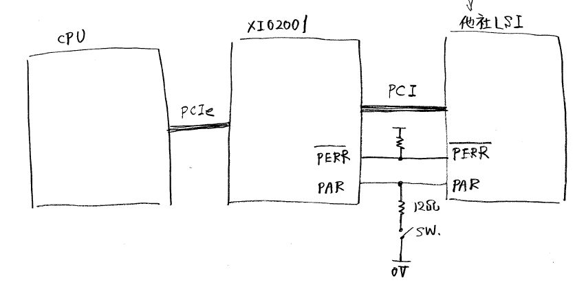
I have a customer working on a prototype board using the XIO2001 - and they are in the process of debugging.
Most features of the device seem to operate without any issues.
However, when they confirmed the behavior when try and instigate the parity alarm, the XIO2001 register shows parity error, but the PERR pin does not get driven LOW. It stays in Hi-Z.
What is the correct setup to get PERR to be driven LOW during such an error?
These are the register settings as seen from the CPU (PCIe) side.
70800000 : 104C 8240 0007 0010 0000 0604 0000 0001 .L.@............
70800010 : 0000 0000 0000 0000 0000 0000 0101 02A0 ................
70800020 : 0000 0000 0001 0001 0000 0000 0000 0000 ................
70800030 : 0000 0000 0040 0000 0000 0000 00FF 0001 .....@..........
70800040 : 480D 0000 0000 0000 5001 0603 0008 0040 H.......P......@
70800050 : 7005 0088 0000 0000 0000 0000 0000 0000 p...............
70800060 : 0000 0000 0000 0000 0000 0000 0000 0000 ................
70800070 : 0010 0072 8002 0000 2000 0010 4C11 0006 ...r.... ...L...
70800080 : 0000 1011 0000 0000 0000 0000 0000 0000 ................
70800090 : 0000 0000 0000 0000 0000 0000 0000 0000 ................
708000A0 : 0000 0000 0000 0000 0000 0000 0000 0000 ................
708000B0 : 0000 0900 0000 001F 0000 0000 0000 0000 ................
708000C0 : 0001 0208 0108 0012 2000 3214 0000 0000 ........ .2.....
708000D0 : 0000 0000 025F 8600 0000 0000 0040 0000 ....._.......@..
708000E0 : 0000 0000 0000 0000 0443 0008 007F 01C0 .........C......
708000F0 : 0000 0000 0000 0000 0000 0000 0000 0000 ................
70800100 : 0001 0001 0000 0000 0000 0000 2031 0006 ............ 1..
70800110 : 0000 0000 2000 0000 00A0 0000 0000 0000 .... ...........
70800120 : 0000 0000 0000 0000 0000 0000 0000 0000 ................
70800130 : 17A8 0000 1340 0000 0000 0000 0000 0000 .....@..........
70800140 : 0000 0000 0000 0000 0000 0000 0000 0000 ................
This is the method they are taking:
- The PCI bus cycle's data phase is set so that data with PAR=H can be written in the LSI (PCI side of the XIO2001)
- The CPU leads with long (32bit) data so that the address phase of the PCI bus cycle is PAR = L
- With the CPU leading, a switch connects the PAR pin (connected to XIO2001 and LSI) to 0V via 12Ω resistor - forcing a parity error
- Register 1E becomes 83A0, but the PERR signal stays Hi-Z
To confirm
- They write the LSI with data so PAR = L, then they do the same setup as above with the switch. 1E register area becomes 02A0, and PERR stays Hi-Z. This is expected behavior.