Because of the Thanksgiving holiday in the U.S., TI E2E™ design support forum responses may be delayed from November 25 through December 2. Thank you for your patience.

This thread has been locked.

If you have a related question, please click the "Ask a related question" button in the top right corner. The newly created question will be automatically linked to this question.

TCAN4550-Q1: Use a stand alone transceiver

Part Number: TCAN4550-Q1
Other Parts Discussed in Thread: TCAN4550EVM, TCAN4550

I enable the GPIO1 and GPO2 as RXD_INT_CAN and TXD_INT_CAN by adding TCAN4x5x_Device_EnableTestMode(TCAN4x5x_DEVICE_TEST_MODE_PHY).

I have test it on the TCAN4550EVM. So I made a pcb to test it, but the RXD_INT_CAN and TXD_INT_CAN doesn't have any signal.

Do you have any idea about this?

  • Hello Ted,

    The test mode you have configured removes the CAN FD Controller from the system and uses the TCAN4550 as a standalone transceiver.  You will need to provide the TXD signal to the GPIO1 pin, the EN signal to the nINT pin, and the RXD signal should reflect the CANH, CANL, and TXD signal on the GPO2 pin.  This test mode is shown as Figure 28 in the datasheet which I have highlighted below.  Is this your intended configuration? If so, you should see the GPO2 pin reflect the RXD signal when you supply a TXD signal on the GPIO1 pin and the nINT pin has a good EN signal.  If this is not the case, can you provide a schematic of your board and a diagram of your test setup for my review?

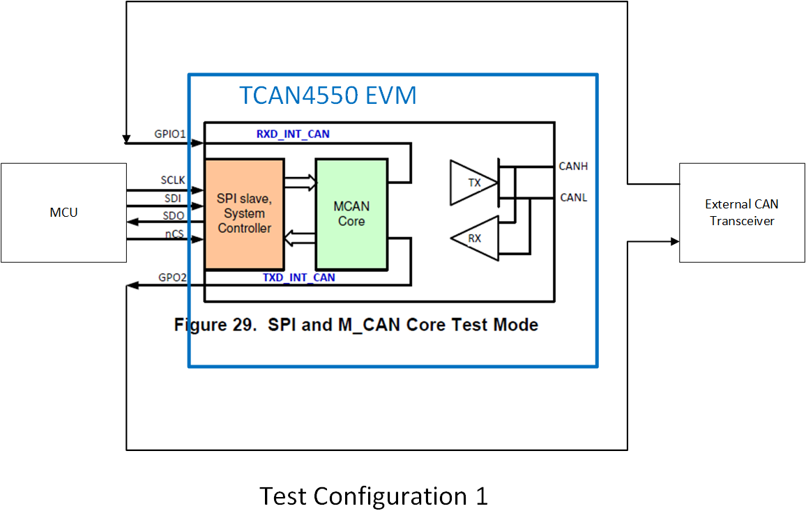
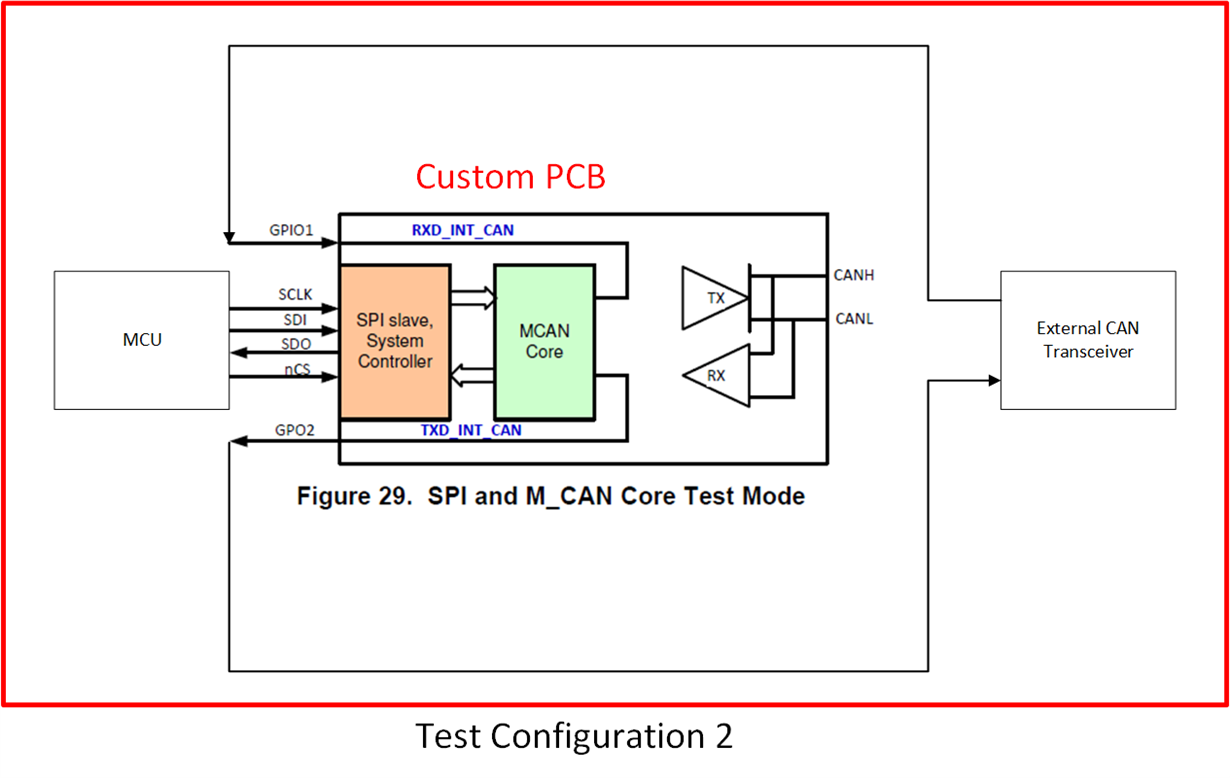
    If you were instead wanting to connect an external transceiver to the TCAN4550's CAN FD Controller, then you want the test mode shown in figure 29.  This would correspond with the following function call:

    TCAN4x5x_Device_EnableTestMode(TCAN4x5x_DEVICE_TEST_MODE_CONTROLLER)

    If you connect an external transceiver to the GPIO1 and GPO2 pins in this mode, you should be able to see the signals on the CANH and CANL pins as you try to send messages.

    Regards,

    Jonathan

  • Hi Jonathan,

    I past a wrong function, My project is connect an external transceiver to the TCAN4550,

    I add the function TCAN4x5x_Device_EnableTestMode(TCAN4x5x_DEVICE_TEST_MODE_CONTROLLER) after Init_CAN().

    This function was work fine when I use TCAN4550EVM, but in my schematic it doesn't work.

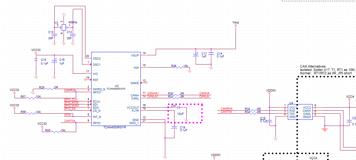
    This is the part of tcan4550 and external transceiver.

    In my test, The external transceiver can receive data to GPIO1(RXD_INT_CAN) but TCAN4550's CAN FD Controller doesn't receive it. Sending data from TCAN4550's CAN FD Controller, GPIO2(TXD_INT_CAN) doesn't have any data output. I get BUS_OFF and Error_passive status from TCAN4550.

    Is there any way can check the function or my schematic have wrong?

    Regards,

    Ted

  • Hi Ted,

    Thank you for providing the schematic for review. I have the following comments:

    -        The RST (reset) pin is floating. There is a weak pulldown resistor in the device, but it is possible that this is not strong enough keep the device from entering the reset condition if there is some noise in the system. It is recommended to add an external source to this pin or an external pulldown resistor as well.

    -        The WAKE pin is floating. When this pin is not used, it is recommended to directly connect it to either VSUP or GND to prevent it from changing state that can cause an interruption to the TCAN4550.

    -        The FLTR pin requires a capacitor which is used to stabilize the internal 5V LDO and a recommended value of 330nF (0.33uF) is recommended. The 0.1uF capacitor currently used should be increased in value.

    -        The WKRQ_N pin is an output pin that is shorted to GND through a 0-ohm resistor. R29 should be removed.

    -        The CAN pins are unterminated and will require a 60-ohms of resistance placed between the terminals, either on the board, or on the bus through the typical 120-ohm resistors placed at each end of the CAN bus. CAN protocol requires 60-ohms of impedance between these pins for communication. If you do not intend to use the internal transceiver this is ok. But you have not shown the portion of the schematic that contains the transceiver you are using, and it will require the termination.

    -        I see that a TCAN4550 VIO voltage of 3.3V, and a VDD voltage of 5V used on U4. This mismatch could prevent the RX and TX digital data from crossing the required thresholds of the two devices.

    -        The 30pF value of the C12 and C13 capacitors on the crystal appear too large based on my past experience. I do not know what the requirements of this specific crystal may be, but values closer to 8pF are what I commonly see. If these capacitors are too small or too large, there may be conditions that cause the oscillation to stop or not start at power up. These values should be checked and adjusted if necessary.

    Some of the schematic comments could contribute to your communication problems, but if you are able to read and write registers in the TCAN4550, most of these may be suggestions for improvements.

    The configuration settings you use with the TCAN4550 EVM should also be compatible with the board you have developed. However, when you state that you get a Bus Off and Error Passive status from the TCAN4550, this tells me a lot of useful information. You will need to have a second operational CAN Module connected to your TCAN4550 board through the CANH and CANL lines that will “Acknowledge” the CAN message you are trying to send.

    If a second node is not connected properly, the TCAN4550 will try to transmit the message that could result in a TX Fault and increase the TX Error Count. It will then try to transmit the message again until it is successfully transmitted or the error count maximum threshold is reached. Once this error count reaches the maximum value, the device will enter the Bus Off state and disable itself from any activity on the CAN bus and set the INIT bit to ‘1’. The MCU will need to set the INIT bit back to ‘0’ before it can participate in CAN activity.

    Unless the Disable Automatic Retransmission (DAR) bit is set, the device will quickly enter the Bus Off state if there is a configuration error on the bus. I suspect that following the initial configuration, the first message you try to transmit is causing the TX error count to increase rapidly and the device enters the Bus Off where you are stuck. If you connect a scope probe on the TX signal during you startup, are you able to see this initial activity on the TX pin as it tries to transmit the first message?

    You can try to disable the automatic retransmission by setting the DAR bit to ‘0’ so that it only tries to transmit the message a single time. And you may want to enable the External Loopback feature for now so that it will treat the message you are transmitting on the TX pin as a valid Received message on the RX pin and ignore the Acknowledge that comes from a second message. This is done through the LBCK bit in the Test register 0x1010.

    Can you check if any of the schematic recommendations make a difference? Can you capture any activity on the TX pin with a scope immediately following the initialization when that first message is transmitted? Can you try to set the DAR and or LBCK bits to see if we can prevent the device from entering the Bus Off state?

    Regards,

    Jonathan

  • Hi Jonathan,

    I took a moment to modify the schematic and check the configuration settings I use with the TCAN4550EVM.

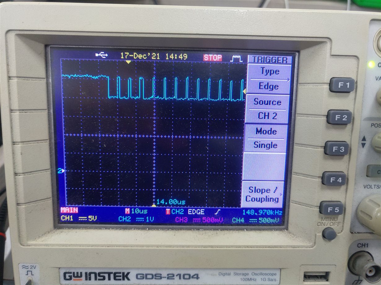
    I have an CAN BUS analyzer, so I send messages to test TCAN4550 with its own transceiver. The data is correct send and receive. But when I send message by external transceiver, the TX pin didn't have any activity. When receiving message, the external transceiver send data to RX(GPIO1) pin and I capture as follow.

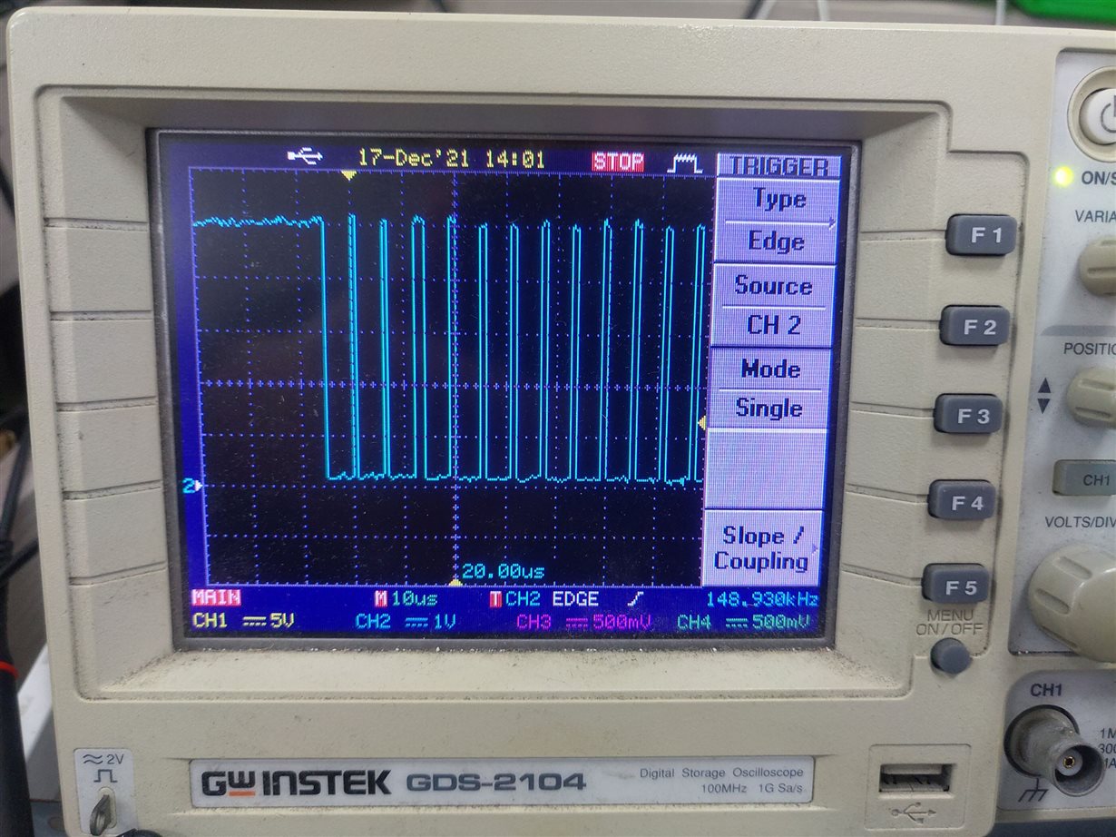
    I think this is not correct, so I cut the RX line to TCAN4550 then I get the waveform like this.

    The waveform looks correct. Now I don't know why the waveform is changed when RX pin connect to external transceiver. RX pin didn't have an external pulldown and pullup resistor.

    Regards,

    Ted

  • Hi Ted,

    Thanks for the waveforms.  I noticed something off with the voltage levels.

    What is the part number of the isolated CAN transceiver you are using (U4)? Will it work at 3.3V on the TCAN4550 side for the TX and RX signals?

    You are using a VIO voltage of 3.3V with a 10k pullup resistor on the RX and TX signals and the TCAN4550 is expecting a digital IO voltage level of 3.3V for both the TX and RX signals.  However you are using 5V for the VCC1 voltage of the isolated CAN transceiver, therefore I expect it to use 5V for the digital IO levels on RX and TX.

    There may be a problem with the two different voltage levels.  Are you using the same Isolated CAN transceiver with the EVM when you are doing the test?  If so, is it working with the EVM with the two different voltage levels?

    I don't think the 10k pullup resistors should be needed in this case, and you may try removing them to see if it helps the signals reach the proper amplitudes.

    Regards,

    Jonathan

  • Hi Jonathan,

    The waveforms is captured after I change the VIO voltage to 5V and remove the 10k pullup resistors on RX. The voltage level of  TCAN4550 and isolated CAN transceiver is the same.

    The isolated CAN transceiver I am using ADM3050. The CAN transceiver is different when i test with EVM. I also test the same can transceiver in my pcb, but the waveform is the same.

    Regards,

    Ted

  • Hi Ted,

    I would like to verify my understanding of your test setup to make sure I am not missing anything.  I have drawn two diagrams for you verify.

    It is my understanding that you have done a test with an MCU, an TCAN4550 EVM, and an external CAN transceiver as shown in the following figure.  It is also my understanding that your firmware correctly configures the TCAN4550 to send and receive CAN messages through this external transceiver.  Is that correct?

    It is also my understanding that you then created your own custom PCB according to the following figure.  I do not know if if the MCU is on this board or whether it is still separate, but the TCAN4550 and the external transceiver are on your PCB and you have shared the schematics for my review.  Is that correct?  And it is my understanding that you tried to use the exact same firmware that you used in the first test configuration using the TCAN4550 EVM but this is NOT working correctly even though no functional changes to the schematic or firmware were made.  Is that correct?

    Therefore if the same firmware is used for both and the firmware correctly works on an EVM with an external transceiver, this would lead to some form of hardware or schematic difference.

    But if the same firmware was not used, or I am incorrectly understanding that you have been able to use an external transceiver with the EVM and instead you have only been successful using the TCAN4550's internal transceiver, then this would point to a firmware issue.

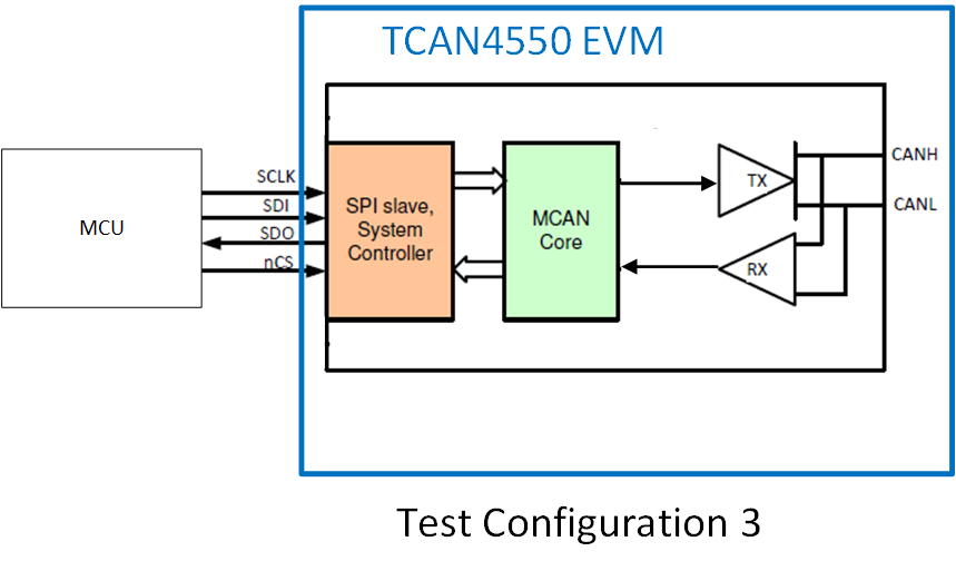
    Finally it is my understanding that you have been able to get the TCAN4550 to work using the internal transceiver as show in the following figure.  Is that correct?

    So Test Configuration 1 and 3 work, but Test configuration 2 does not.  Do I have a correct understanding of everything?  If not, please correct anything I do not have correct.

    Regards,

    Jonathan

  • Hi Jonathan.

    The test Configuration is correct, The MCU is also on the same PCB. Only Test Configuration 2 doesn't work

    Regards,

    Ted

  • Hi Ted,

    Thanks for your confirmation, and I apologize for not following up with you on Friday.  There are really three main things you need for this setup that I think we need to verify.  We need to make sure the supply and IO pins are at the proper voltage levels.  We need to make sure the clock is functioning.  And we need to make sure the SPI communication is correct.

    Can you verify the voltage levels on the following pins: VSUP, VIO, VCCOUT, RST, INH, nWKRQ, GPIO1, and GPO2?  This will help me determine if any of the pins are not at expected levels that would point to the error.

    Can you add into your MCU firmware routine some functions to read back the configuration register values?  This will test both the Clock and SPI communication.  If the clock does not work, the device will not return the values on the SPI bus.  And if the read back values do not match with the expected values, then it is possible the device is not being placed into the proper test mode, either through a firmware setting or schematic element that has been overlooked, or through some problem with the SPI signals.

    Can you read back the following registers:

    TCAN4550 Device Configuration Registers:

    0x0000 (Device ID, this will work even if the CLK is not working and only uses the SPI clock)

    0x000C (Status Reguster)

    0x0800 (Modes of Operation and Configuration Register)

    0x0820 (Interrupt Flags)

    0x0824 (MCAN Interrupt Flags)

    MCAN Controller CAN FD Configuration Registers:

    0x100C (Data Bit Timing & Prescaler Register

    0x1018 (Control Register)

    0x101C (Nominal Bit Timing & Prescaler Register

    0x1040 (Error Counter Register)

    0x1044 (Protocol Status Register)

    0x1048 (Transmitter Delay Compensation Register)

    0x1050 (Interrupt Register)

    These registers will help me understand how you have configured the device and any status bits that may be getting set that would point to why it is not working properly.

    Regards,

    Jonathan

  • Hi Jonathan,

    I got the communicate work by setting the TCAN4x5x_DEV_CONFIG from Init_CAN().

    If I set "Keep Sleep Wake Error" disabled, The waveform of Rx will show as the wrong one.

    When "Keep Sleep Wake Error" enabled, The external isolation transceiver can work fine with TCAN4550 and the waveform is correct.

    I don't know why disable the "Keep Sleep Wake Error" cause the voltage level wrong, Is there a detail information about this?

    Regards,

    Ted

  • Hi Ted,

    Ok, it sounds like we are making some progress, but this is an interesting observation.  I believe what you are referring to sets the SWE_DIS bit, or bit 1 of register 0x0800.  Is this correct?  If so, I would have expected the opposite behavior.

    The SWE timer is one of the 3 Failsafe features of the TCAN4550 and discussed in section 8.4.5 of the datasheet. Basically when the device powers on, or sees a Wake Up event, it enters Standby Mode and starts a 4 minute timer.  If the device doesn't get configured and placed into Normal Mode before that 4 minute timer expires, then it assumes that the Wake Up event was erroneous and the device enters Sleep Mode again.  This is usually problematic for initial development because it is easy to have a 4 minute pause where the device reverts back to Sleep Mode without your knowledge.  Usually I have to recommend disabling this feature.

    However, your telling me that the opposite is true and that disabling this feature is causing a problem.  I know of no other purpose or dependency of this bit that would cause you to not communicate with an external transceiver.  Are you configuring the device immediately after power up, or is there some potential timing delay?

    Are you disabling the watchdog timer and or the general Failsafe Enable bit as well? 

    With the Sleep Wake Error disabled, can you read the configuration and status registers while the device is not working correctly to see whether it has thrown any error flags and or reverted to a sleep or standby mode as a result of a failsafe timeout?

    Regards,

    Jonathan

  • Hi Jonathan,

    Here is the settings in my code.

        /* Configure the TCAN4550 Non-CAN-related functions */
        TCAN4x5x_DEV_CONFIG devConfig = {0};
        devConfig.SWE_DIS = 0;
        devConfig.DEVICE_RESET = 0;
        devConfig.WD_EN = 0;
        devConfig.nWKRQ_CONFIG = 0;
        devConfig.INH_DIS = 0;
        devConfig.GPIO1_GPO_CONFIG = TCAN4x5x_DEV_CONFIG_GPO1_MCAN_INT1;
        devConfig.FAIL_SAFE_EN = 0;
        devConfig.GPIO1_CONFIG = TCAN4x5x_DEV_CONFIG_GPIO1_CONFIG_GPO;
        devConfig.WD_ACTION = TCAN4x5x_DEV_CONFIG_WDT_ACTION_nINT;
        devConfig.WD_BIT_RESET = 0;
        devConfig.nWKRQ_VOLTAGE = 0;
        devConfig.GPO2_CONFIG = TCAN4x5x_DEV_CONFIG_GPO2_NO_ACTION;
        devConfig.CLK_REF = 1;
        devConfig.WAKE_CONFIG = TCAN4x5x_DEV_CONFIG_WAKE_DISABLED;

    When I set "SWE_DIS=1" the external transceiver can not communicate with tcan4550.

    I configure the TCAN4550 as quickly as possible after power up, but sometimes I change the settings like filter and CAN bus speed after minutes.

    I read the configuration and status registers while the device is not working correctly.

    The configuration registers (0x0800) is 0x00000008 and status registers (0x000C) is 082004A3. I use TCAN4x5x_Device_ReadMode to read the mode, the mode still in NORMAL.

    Regards,

    Ted

  • Hi Ted,

    Thanks for the configuration and status register values.  I see from the status register that you are getting SPI errors.  This is caused by the device receiving too few or too many clock pulses (or bits) in a SPI transaction.  As a safety feature, the TCAN4550 counts the number of SCLK pulses to ensure that the communication ends on a byte boundary.  Each register transaction is a 32 bit word and therefore if the there are not exactly 32 bits in the transaction, the TCAN4550 will flag that transaction as an error and discard the data because it's validity cannot be trusted.  An interrupt bit is also generated for this error so that the MCU is informed about the SPI Error and repeat the transaction.

    The Configuration register 0x0800 value of 0x00000008 also seems incorrect for your test mode.  This indicates that the only bit set is the Watchdog Enable bit WD_EN.  I would expect other bits set such as the Test Mode Enable (bit 21) the Mode Select (bits 7:6), etc.

    It is possible that there is either an error with your SPI communication that is resulting from some form of protocol error in the MCU function or a signal integrity error that has noise or reflections on the SCLK line that causes the TCAN4550 to count extra clock pulses resulting in an incomplete configuration. 

    Please monitor the status and interrupt registers for the SPI errors, read back all the registers to verify they were configured with the proper values.  If possible check the SPI signals with a scope to check for signal integrity errors.

    Regards,

    Jonathan

  • Hi Jonathan,

    I have a mistake, I reversed the two register values.

    The configuration registers (0x0800) is 0x082004A3 and status registers (0x000C) is 0x00000008.

    Regards,

    Ted

  • Hi Ted,

    Thanks for the clarification, that makes more sense.  Your status register still shows that at the time you were reading the register that there was an internal multiple transfer mode access in progress.  But without additional information about the other device registers and your MCU SPI activity, I can't make any conclusions on what that might mean in our current debug efforts.

    I know you have said that communication works when you use the EVM.  But can you confirm the behavior on the EVM with your current firmware settings when you enable and disable the SWE_DIS bit?  Does it work with both settings?  I want to confirm whether this is still a board specific issue with the settings and I would expect that as long as you did not allow the timer to timeout, that the EVM would work in test mode for either value of the SWE_DIS bit.

    Can you also read back and provide the final values of the other registers I have previously requested?  Also, could you check the voltage levels on the requested pins?  The additional information will be really helpful in understanding what else might be going on with the device.

    As I've said, I do not know of any dependency with the SWE_DIS bit and the Test Modes.  If you can provide the additional information about the device's configuration and status/interrupt bits, I can consult with one of our digital designers to verify the device configuration and expected behavior.  Is this something you can provide?

    I hope you have a Happy New Years!

    Regards,

    Jonathan

  • Hi Jonathan,

    I test the same code on the EVM, the result is the same.

    I read the register when I set the SWE_DIS bit.

    0x000C (Status Reguster) 0x00000008
    0x0800 (Modes of Operation and Configuration Register)  0x082004A3
    0x0820 (Interrupt Flags)  0x00000000
    0x0824 (MCAN Interrupt Flags) 0x00010000
    0x100C (Data Bit Timing & Prescaler Register 0x00800200
    0x1018 (Control Register) 0x00000100
    0x101C (Nominal Bit Timing & Prescaler Register 0x06010E03
    0x1040 (Error Counter Register) 0x00000000
    0x1044 (Protocol Status Register) 0x0000070F
    0x1050 (Interrupt Register) (Protocol Status Register) 0x00010000

    After sending one message, the register value become as follow.

    0x000C (Status Reguster) 0x00000008
    0x0800 (Modes of Operation and Configuration Register)  0x082004A3
    0x0820 (Interrupt Flags)  0x00000082
    0x0824 (MCAN Interrupt Flags) 0x0B810000
    0x100C (Data Bit Timing & Prescaler Register 0x00800200
    0x1018 (Control Register) 0x00000101
    0x101C (Nominal Bit Timing & Prescaler Register 0x06010E03
    0x1040 (Error Counter Register) 0x001F00F8
    0x1044 (Protocol Status Register) 0x000007E5
    0x1050 (Interrupt Register) (Protocol Status Register) 0x0B810000

    If I didn't set the SWE_DIS bit, the register value is

    0x000C (Status Reguster) 0x00000008
    0x0800 (Modes of Operation and Configuration Register)  0x082004A1
    0x0820 (Interrupt Flags)  0x00000000
    0x0824 (MCAN Interrupt Flags) 0x00010000
    0x100C (Data Bit Timing & Prescaler Register 0x00800200
    0x1018 (Control Register) 0x00000100
    0x101C (Nominal Bit Timing & Prescaler Register 0x06010E03
    0x1040 (Error Counter Register) 0x00000000
    0x1044 (Protocol Status Register) 0x00002708
    0x1050 (Interrupt Register) (Protocol Status Register) 0x00010000

    Regards,

    Ted

  • Hi Ted,

    Thanks for the additional information. It does appear that simply setting the SWE_DIS bit causes the transmission to fail that eventually leads to an overrun of the Transmit Error Counter which forces the device to enter a Bus Off Condition.  Because the device will automatically try to re transmit failing messages, it can be hard to tell if there is any activity on the TXD signal. 

    Can you disable the automatic re transmission by setting the DAR bit in the Control Register to '1'?  This is bit 6 of register 0x1018.  This will cause the device to only transmit the message once regardless of an acknowledgement.  This will allow you to transmit the message up to 255 times before the TEC count reaches the maximum value of 255 causing a Bus Off condition and allow additional time to make observations with a scope, etc.

    Do you also see any activity on the TXD line before the device enters the Bus Off condition?

    I am consulting with our digital design team for verification and comment on your observations and will follow up with you on those soon.

    Regards,

    Jonathan

  • Hi Ted,

    I was able to confirm with our digital design team that there is in fact an internal conflict with the SWE_DIS timer and Test Mode in your configuration.  Because this is technically a test mode, where internal signals are re-routed through the device, some reuse of resources is required.  In this case it looks like disabling the SWE timer creates a conflict with the GPIO pin configuration.

    I'm sorry it took so long to get the root cause, but the register values you provided were very helpful in identifying this internal conflict.  It looks like you will not be able to disable the SWE timer in your application. This just means you will have to configure the registers within 4 minutes of powering up the device to prevent it from transitioning into Sleep Mode.  If it does go into Sleep Mode, any of the Wake Up methods can be used to wake it up, restart the timer and place it into Normal mode.

    Regards,

    Jonathan