This thread has been locked.

If you have a related question, please click the "Ask a related question" button in the top right corner. The newly created question will be automatically linked to this question.

TCA9548A-Q1: I2C interface issue

Part Number: TCA9548A-Q1
Other Parts Discussed in Thread: TCA9548A

Hi Team,

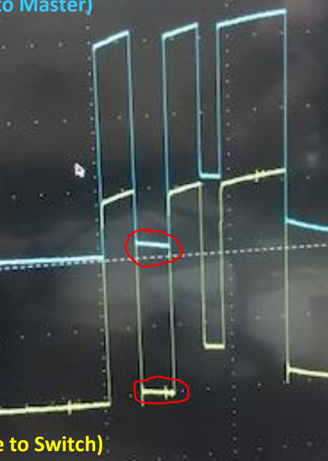
I'd like to ask you about I2C interface issue of this device. There is no problem when SDA is sent from master to slave through switch(TCA9548A-Q1), but there is an issue that the level of ACK signal is increased from less than 1V to more than 1V when sending in the opposite direction only. Please check the attached file below and let me know how to fix it.

TCA9548A-Q1_I2C interface issue.pdf

Regards,

  • Please ensure that you do not measure in AC mode. What are the actual voltages? The on-resistance should be small enough that there is not much of a voltage drop over the switch.

  • Jeffrey,

    I'm curious what VOL you are applying on the responder side, so I would like to know the actual voltages as well.

    Also, how many channels of this device are activated during this test? Is it just the channel being tested, or are all four channels connected?

    Best,

    Danny

  • Hi Danny,

    The voltage division is 1V/div, so actual high level of SDA is around 3.3V. The VOL(max) of responder side is needed to check to my customer.

    As I inform you on attached file, test channel is only between master(Pin 19/20) and slave(Pin 1/2). Please check it.

    Regards,

  • Jeffrey,

    The reason that Clemens and I ask for specific numbers is because there could be a few different causes for this behavior, but it is hard to tell what the most likely cause is without seeing the specifics.

    If the blue line is what is being driven by the controller, then it would not make sense for the yellow line to show occasionally lower voltages than the blue line while the controller is driving, as I see here for example:

    One possible cause for this behavior is if the VOL of the ACK is actually higher than it appears in the image (i.e. over 1 V). If this is the case, then the ACK could be close to Vpass, therein causing RDS_on to be higher. This is why specific voltage readouts would help rule out this possible cause.

    Also, could you share the capacitance characteristics of your bus?

    Lastly, I understand that you are testing one channel. I want to clarify how many channels of the TCA9548A-Q1 are activated during the test. In other words, what is the value stored in the control register? Is it 0xFF?

    Best,

    Danny

  • Hi Danny,

    I understood your specific requirements. ACK signal of SDA looks a little weird, so my customer is debugging about that. Let me check your requirements.(voltage, Vol, capacitance, etc)

    I'd like to explain on the configuration of master and slave. The master is a MCU and the slave is a deserializer like DS90UB954. As you know if the master send the signal(SDA, SCL) to the slave through switch, the slave send the return signal(SDA, SCL) including ACK to the master. So "Slave to Switch" and "Switch to Master" mean the return signal to the master. And I think that Vol of I2C bus is under 1V because Vol of most deserializer is around 0.4Vmax to 0.5Vmax.

    The control register value is 0x01 and just channel 0 is activated.

    Regards,

  • Jeffrey,

    Jeffrey Chung1 said:

    The control register value is 0x01 and just channel 0 is activated.

    This is good. I wanted to make sure the other channels were not connected at the same time.

    Jeffrey Chung1 said:

    I'd like to explain on the configuration of master and slave. The master is a MCU and the slave is a deserializer like DS90UB954. As you know if the master send the signal(SDA, SCL) to the slave through switch, the slave send the return signal(SDA, SCL) including ACK to the master. So "Slave to Switch" and "Switch to Master" mean the return signal to the master. And I think that Vol of I2C bus is under 1V because Vol of most deserializer is around 0.4Vmax to 0.5Vmax.

    Thank you for clarifying.

    Without specific voltages, I am not able to see if we are observing a similar voltage drop the opposite direction when the controller is transmitting the bulk of the SDA data to the responder. Improperly assuming the VOL is 0 V for both measurements could lead to an overrepresentation of how big the voltage difference for the ACK pulse is. This is why it would be helpful to get some precise numerical measurements.

    Jeffrey Chung1 said:

    I understood your specific requirements. ACK signal of SDA looks a little weird, so my customer is debugging about that. Let me check your requirements.(voltage, Vol, capacitance, etc)

    Sounds great, please follow up here when you hear back!

    Best,

    Danny