This thread has been locked.

If you have a related question, please click the "Ask a related question" button in the top right corner. The newly created question will be automatically linked to this question.

SN75DPHY440SS: SN75DPHY440SS: schematic check

Part Number: SN75DPHY440SS

Hi team,

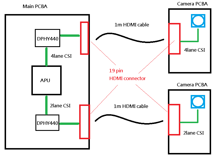
I using SN75DPHY440SS in my platform for dual CSI-2 connection with external camera module by HDMI cable(1m),

my design block diagram as below

This is my circuit as below, I swapped data lane because PCB layout routing, but hope you could also double check on it. Thanks.


  • Hi,

    Please have the pullup/pulldown option on EQ, ERC, Pre, and VSADJ. The configuration pins each have internal pull-up and pull-down resistors of 100 kΩ each. Thus, the recommendation is an external pull-up/pull-down resistors of about 10 kΩ each, to meet the requirement of the threshold levels for the VIL and VIH.

    Lane 0 is a special lane. With Lane 0 path (DA0P/N and DB0P/N) supporting bi-directional LP signaling, it is very important that DB0P/N LP TX is connected to an unterminated LP RX.  

    Thanks

    David

  • Hi David,

    Thanks for your reply,

    I'll add 10 kΩ pullup/pulldown option on EQ, ERC, Pre, and VSADJ.

    For 4 lane group(2lane too) I change the lane order different DPHY440  pin define order is OK?

    For 2 lane group, your mean is when I changed the lane order, I need connect DA0 N/P to ground(DB0 floating?) like refer 2 lane applications in datasheet page22 ?

  • Hi,

    My comment on lane 0 applies in the 4 lane group because I saw RD3 is connected. So you have to make sure the DB0P/N LP TX is connected to an unterminated LP RX. Otherwise you can use I2C to disable lane 0 LP and force it to be HS only.

    Try following for enabling lane0 HS path:

    Enable HS path for Lane 0 only:

    Write Register 0x50 with 8’h01 //Override enable for HS TX path

    Write Register 0x51 with 8’h01 //HS TX path enabled.

    Write Register 0x61 with 8’h00  // Disable LP path.

    Write Register 0x70 with 8’h01  //Override enable for HS RX path

    Write Register 0x71 with 8’h01  // HS RX path enabled.

    Bit 0 is lane 0

    2 lane group lane order is ok as long as output lane order matches input lane order.

    Thanks

    David

  • Hi David,

    Thanks for your reply,

    I modified schematic for 4 lane group, adding I2C(1.8V) and 10 kΩ pullup/pulldown option on EQ, ERC, Pre, and VSADJ.


    For DBx I connect to APU(Rx), for DAx is connect to Camera(Tx), does it OK for I using DB0?

    I think my camera will stay in HS-mode always, so that we need using I2C control DPHY440 too ?


  • Hi,

    The schematic looks ok. 

    To enable the DPHY440 HS mode only, you have to use the I2C to control the DPHY440.

    Thanks
    David

  • Hi David,

    I got it, Thanks for your reply, and support.