Part Number: SN65DP159
It may not be output at startup or when changing the mode setting (APPLY_RXTX_CHANGES). If it is not output, it will be output by repeating
APPLY_RXTX_CHANGES, but if APPLY_RXTX_CHANGES is set during output, it may not be output frequently.
The operating environment is as follows.
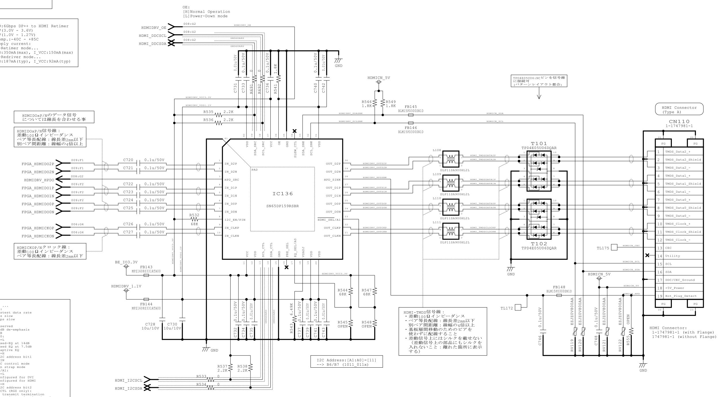
1) The circuit diagram is attached.
2) The input to DP159 is the HDMI IP output of Xilinx.
3) The VCC / VDD / OE power-up sequence complies with the regulations.
4) The tested images are 1080P59.94 and 2160P59.94, both of which occur.
5) The register value of bank 1 differs depending on whether it is output or not (attached).
6) Reflecting the settings in PD_EN is less frequent than APPLY_RXTX_CHANGES, but it does not solve the problem.
It would be helpful if you could give me some advice.
By the way, if I can check the output status with the hidden register of DP159, I can set APPLY_RXTX_CHANGES while checking the flag. Is there such a flag?
2160P output (normal register read value):
DP159 register dump [BANK:00]
ADDR[00] = 44 50 31 35 39 20 20 20 01 06 33 9A 49 00 00 0F
ADDR[10] = 00 00 00 00 00 80 00 20 00 00 00 00 85 0D 00 00
ADDR[20] = 0A 00 00 00 00 00 00 00 00 00 00 00 00 00 00 00
ADDR[30] = 00 00 00 00 00 00 00 00 00 00 00 00 00 00 00 00
ADDR[40] = 00 00 00 00 00 00 00 00 00 00 00 00 00 00 00 00
ADDR[50] = 00 00 00 00 00 00 00 00 00 00 00 00 00 00 00 00
ADDR[60] = 00 00 00 00 00 00 00 00 00 00 00 00 00 00 00 00
ADDR[70] = 00 00 00 00 00 00 00 00 00 00 00 00 00 00 00 00
ADDR[80] = 00 00 00 00 00 00 00 00 00 00 00 00 00 00 00 00
ADDR[90] = 00 00 00 00 00 00 00 00 00 00 00 00 00 00 00 00
ADDR[A0] = 00 00 00 00 00 00 00 00 00 00 00 00 00 00 00 00
ADDR[B0] = 00 00 00 00 00 00 00 00 00 00 00 00 00 00 00 00
ADDR[C0] = 00 00 00 00 00 00 00 00 00 00 00 00 00 00 00 00
ADDR[D0] = 00 00 00 00 00 00 00 00 00 00 00 00 00 00 00 00
ADDR[E0] = 00 00 00 00 00 00 00 00 00 00 00 00 00 00 00 00
ADDR[F0] = 00 00 00 00 00 00 00 00 00 00 00 00 00 00 00 00
DP159 register dump [BANK:01]
ADDR[00] = C3 01 3F 00 A0 00 00 00 01 00 00 33 00 00 11 00
ADDR[10] = 0F 30 20 07 01 00 00 00 00 00 00 00 00 00 00 00
ADDR[20] = 00 00 00 00 00 00 00 00 00 00 00 00 00 00 00 00
ADDR[30] = 07 30 08 00 00 00 00 00 00 08 00 08 04 06 00 00
ADDR[40] = 80 80 80 80 C1 00 00 00 FE 3F 7F FF 03 00 21 71
ADDR[50] = 00 00 00 00 00 00 00 00 00 00 00 00 40 40 40 40
ADDR[60] = 00 00 00 00 00 00 00 00 00 00 00 00 00 00 00 00
ADDR[70] = 00 00 00 00 00 00 00 00 00 00 00 00 00 00 00 00
ADDR[80] = 00 10 00 00 00 00 00 00 00 00 00 00 00 00 00 00
ADDR[90] = 00 00 00 00 00 00 00 00 00 00 00 00 00 00 00 00
ADDR[A0] = 00 00 04 00 00 00 00 00 00 00 00 00 00 00 00 00
ADDR[B0] = 5E 82 00 00 00 00 00 00 00 00 00 00 00 00 00 00
ADDR[C0] = 00 00 00 00 00 00 00 00 00 00 00 00 00 00 00 00
ADDR[D0] = 00 00 00 00 00 00 00 00 00 00 00 00 00 00 00 00
ADDR[E0] = 00 00 00 00 00 00 00 00 00 00 00 00 00 00 00 00
ADDR[F0] = 00 00 00 00 00 00 00 00 00 00 00 00 00 00 00 01
2160P output (register read value at abnormal time)
DP159 register dump [BANK:00]
ADDR[00] = 44 50 31 35 39 20 20 20 01 06 33 9A 49 00 00 0F
ADDR[10] = 00 00 00 00 00 80 00 20 00 00 00 00 85 0D 00 00
ADDR[20] = 0A 00 00 00 00 00 00 00 00 00 00 00 00 00 00 00
ADDR[30] = 00 00 00 00 00 00 00 00 00 00 00 00 00 00 00 00
ADDR[40] = 00 00 00 00 00 00 00 00 00 00 00 00 00 00 00 00
ADDR[50] = 00 00 00 00 00 00 00 00 00 00 00 00 00 00 00 00
ADDR[60] = 00 00 00 00 00 00 00 00 00 00 00 00 00 00 00 00
ADDR[70] = 00 00 00 00 00 00 00 00 00 00 00 00 00 00 00 00
ADDR[80] = 00 00 00 00 00 00 00 00 00 00 00 00 00 00 00 00
ADDR[90] = 00 00 00 00 00 00 00 00 00 00 00 00 00 00 00 00
ADDR[A0] = 00 00 00 00 00 00 00 00 00 00 00 00 00 00 00 00
ADDR[B0] = 00 00 00 00 00 00 00 00 00 00 00 00 00 00 00 00
ADDR[C0] = 00 00 00 00 00 00 00 00 00 00 00 00 00 00 00 00
ADDR[D0] = 00 00 00 00 00 00 00 00 00 00 00 00 00 00 00 00
ADDR[E0] = 00 00 00 00 00 00 00 00 00 00 00 00 00 00 00 00
ADDR[F0] = 00 00 00 00 00 00 00 00 00 00 00 00 00 00 00 00
DP159 register dump [BANK:01]
ADDR[00] = C3 01 3F 00 A0 00 00 00 01 00 00 33 00 00 11 00
ADDR[10] = 0F 30 20 07 01 00 00 00 00 00 00 00 00 00 00 00
ADDR[20] = 00 00 00 00 00 00 00 00 00 00 00 00 00 00 00 00
ADDR[30] = 07 30 08 00 00 00 00 00 00 08 00 08 04 06 00 00
ADDR[40] = 80 80 80 80 C1 00 00 00 F8 3F 7F FF 03 00 21 71
ADDR[50] = 00 00 00 00 00 00 00 00 00 00 00 00 40 40 40 40
ADDR[60] = 00 00 00 00 00 00 00 00 00 00 00 00 00 00 00 00
ADDR[70] = 00 00 00 00 00 00 00 00 00 00 00 00 00 00 00 00
ADDR[80] = 00 10 00 00 00 00 00 00 00 00 00 00 00 00 00 00
ADDR[90] = 00 00 00 00 00 00 00 00 00 00 00 00 00 00 00 00
ADDR[A0] = 00 00 04 00 00 00 00 00 00 00 00 00 00 00 00 00
ADDR[B0] = 5E 82 00 00 00 00 00 00 00 00 00 00 00 00 00 00
ADDR[C0] = 00 00 00 00 00 00 00 00 00 00 00 00 00 00 00 00
ADDR[D0] = 00 00 00 00 00 00 00 00 00 00 00 00 00 00 00 00
ADDR[E0] = 00 00 00 00 00 00 00 00 00 00 00 00 00 00 00 00
ADDR[F0] = 00 00 00 00 00 00 00 00 00 00 00 00 00 00 00 01