This thread has been locked.

If you have a related question, please click the "Ask a related question" button in the top right corner. The newly created question will be automatically linked to this question.

DS90UB954-Q1: DS90UB954-Q1

Part Number: DS90UB954-Q1
Other Parts Discussed in Thread: ALP, USB2ANY

Does model (IBIS) provided for the device models capacitance seen by the oscillator that drives XIN/REFCLK pin? If not, what would be the worst case capacitance at this pin? We have a design where several DS90UB954-Q1 devices share the same clock source and we would like to know what would be capacitive load seen by clock source in this particular case. Also, if rise and fall time specification 6ns/6ns at this pin is not met (if clock edges are a bit slower, let's say 8ns), how would that influence device's performance.

  • Hello Goran,

    Yes the 954 IBIS model includes C_Comp and C_Pkg parameters for the XIN/REFCLK pin. We have no supporting data to qualify the device performance outside the scope of the AC electrical specs in the datasheet, but in a corner case, a very slow ramp time could potentially cause an error in the clock edge detection circuitry which could result in a link error, CSI-2 error, or various other unwanted conditions. It is best to ensure that the datasheet specs can be met. Best practice when designing such a system where one clock source is shared between multiple end points is to use a clock fanout buffer. If you need assistance in selecting a fanout buffer, we have several available products that could fit from the TI portfolio as well. 

    Best Regards,

    Casey 

  • Hi Casey,

    Thanks for your answer. I have one additional question. I have a system where we are using several (6) 954 deserializers and occasionally we are noticing  FPD link parity errors (About one error per hour). We are using CSI synchronous mode, and our refclk is 25MHz  We did not see this initially because, by default, parity threshold register is set to 0x0100. After we set it to 0x0001 parity errors started popping up. Does default threshold setting means that some errors are to be expected? If so, what would be expected rate of parity errors on a system that may be qualified as "Good"..

    Regards

    Goran

  • Hello Goran,

    BER is defined by the application, so you would need to make a determination about what sort of BER is acceptable for your system. However from the device qualification standpoint our device targets a BER or 1e-12 or better from the IC design perspective. In practice, the vast majority of applications achieve far better BER than this - 1e-14 or even 1e-15. If you are getting parity errors frequently during only a few minutes of testing, it seems likely the design could be improved. In our qualification testing we do overnight testing to ensure 0 errors are captured for example. 

    First, please check that these are real errors during operation and not errors happening during the initial linking process. So once the link is established, please clear the parity error counter so you reset it to zero. If you are still getting parity errors after this during only a few minutes testing it would be good to check the component design schematics to make sure they match the datasheet recommendations, especially the PoC filtering and noise characteristics if there is PoC implemented. Also you can run the margin analysis tool to see what sort of system margin you have with this design:

    https://www.ti.com/lit/pdf/snlu243

    http://www.ti.com/lit/pdf/SNLA301 

  • Hi Casey,

    Thanks for the provided info. Unfortunately I do not have TI's FPD link evaluation module. What I have is a custom built board. So it looks that I can't use MAP to analyze my FPD links because I don't see how I could connect deserializers on my board  to a PC. So all I could do is to perform this analysis manually (or by writing a program which would do the same thing MAP does). Am I mistaken?

    Best Regards

    Goran

  • Hello Goran,

    You can use MAP with a custom designed board too. You can use an Aardvark or USB2ANY module to connect I2C into your target board, and then link with the ALP GUI via USB. Also you are free to integrate the MAP tool code into your custom SoC/MCU code as well. The code is available in the ALP install folder here:

    C:\Program Files (x86)\Texas Instruments\Analog LaunchPAD v1.57.0010\PreDefScripts\DS90UB954\ub954_margin_analysis_script

    Best Regards,

    Casey 

  • Hi Casey,

    Thank you for your help so far. I actually decided to incorporate margin analysis check into my existing software. I was following description of MAP functionality from the documents you sent me since this was easier than reverse engineering procedure from those scripts  I also decided to mimic manual adaption mode by leaving AEQ adaption mode enabled and setting the minimum and maximum strobe position to the same value. So I am doing the following:

    1. Initialize the system (deserializer, serializer and imager connected to serializer) as I would normally do

    2. Set the same values for SFILTER_MAX and SFILTER_MIN in SFILTER (0x41) 

    3. Set ADAPTIVE EQ BYPASS (0xD4)

    4. Reset digital block without resetting registers

    5. Run the test for 30 seconds.

    6. Check 0x4D[5:2] and 0x4E[5] for errors

    And here is my problem. If I am using described procedure results I am getting don't have much sense (for SFILTER and EQ both set to zero system passes the test which is pretty much impossible). I discovered that in that case deserializer reports that measured frequency is not stable (RX_PORT_STS2 (Address 0x4E) bit 2) and all the error bits are cleared - that is why I was getting the ""Passed" result. When I included RX_PORT_STS2 (Address 0x4E) bit 2 into "Pass/Failed" classification I started to get much more reasonable results. So my question is: Since RX_PORT_STS2 (Address 0x4E) bit 2 was not mentioned in the document describing MAP functionality, is there any other bit that should be included into "Pass/Failed" classification?

    Regards

    Goran

  • Hello Goran,

    For this type of test I would just suggest using the LOCK status and other latching error flags in the 0x4D register rather than the bits in the 0x4E register. Those will give you an easier way to see if you have a link or not, if the link has dropped since the last time you checked the register, or if you are getting parity errors. 

    Best Regards,

    Casey 

  • Hi Casey,

    Thanks for the answer. One more question. Is there a way to check which SFILTER / ADAPTIVE EQ values deserializer is actually using. I am, of course, refering to the case where these values are determined by deserializer automatically.

    Regards

    Goran

  • Hello Goran,

    The current EQ value is located in register 0xD3 and the strobe values are located in 0xD6 and 0xD7 (see this app note for descriptions of 0xD6 and 0xD7): https://www.ti.com/lit/pdf/snla301 

    Best Regards,
    Casey 

  • Hi Casey,

    As you can see I am still working on the same issue. In the meantime we purchased USB2ANY adapter and used it to tweak our own test routines which are a bit faster so they are now producing the same results as Margin Analysis Program. Our tests showed that one some deserializers one FPD channel would perform perfectly while the other would produce far worst margin analysis results. We noticed that the level of noise on pins 3 and 20 is above maximum specified in the datasheet. We are measuring approximately 80mVpp while datasheet states that the maximum allowable level is 25mVpp. Our measurement showed that a single VIA with 25um hole used to connect decoupling capacitor placed at the bottom layer (whereas deserializer is at the top layer) is insufficient and has impedance which is too big. So here is what I would like to know:

    1. How critical is increased noise on pins 3 and 20? Could that explain why one FPD channel works well and the other does not?

    2. PCB example that may be found in 954 datasheet also shows a single VIA for connecting pin 3 to decoupling capacitor which is apparently also at opposite layer from the deserializer. Are current impulses at pins 3 and 20 really that big and fast to produce a few tens of millivolts of voltage drop across a single VIA? Since the same behavior is present across all the boards and deserializers VIA issue does not seem to be production related.

    Best Regards

    Goran

  • Hello Goran,

    1. All datasheet specifications including noise tolerance are critical to ensure device performance. If the design does not meet the datasheet then I would expect degraded performance. 

    2. The issue is probably not related to DC impedance based on there being one via. The issue is most likely related to the characteristic impedance of the transmission line based on your PCB stackup, hole size, trace widths, material selection, etc. The FPD traces target a 100 ohm differential/50 ohm single ended characteristic impedance, and the impedance continuity is critical to ensure reflections are minimized in the high speed channel. You should not use more than one via to route the signal because then you would significantly interrupt the trace geometry and change the characteristic impedance. You will need to understand within your particular PCB parameters how to optimize the layout, via sizing, etc. to maintain 100 ohm differential impedance which may also involve doing some simulations in an EM solver like Ansys for example. If you post a picture of your layout, we can also suggest optimizations based on our best practice

    Best Regards,

    Casey 

  • Hi Casey,

    Thanks again for your assistance. 

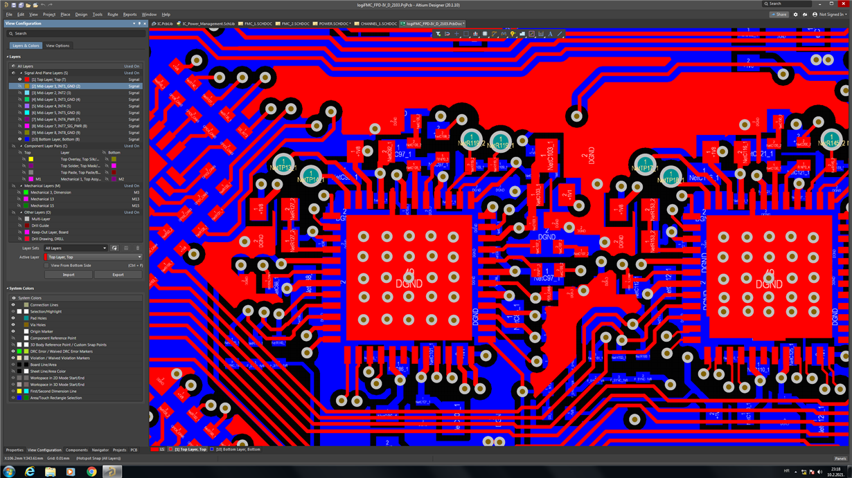
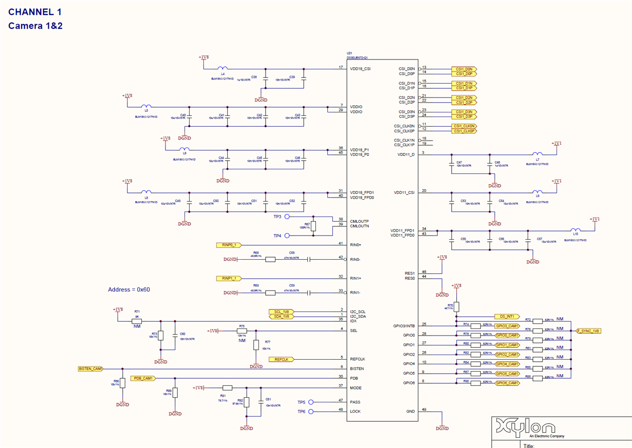
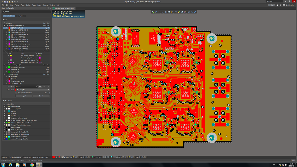
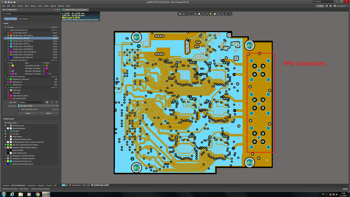
    We were also suspecting that the problem might be related to FPD link PCB trace impedance or some impedance discontinuities that may be present. Yesterday I did an experiment using deserializer where one channel works well and the other does not. I connected 1m long, 50 ohms coaxial Leoni Dacar 301 cable directly to deserializer effectivly bypassing the PCB trace completely (100nF DC blocking capacitor was, of course, present).. PCB trace DID NOT not remain connected to DC blocking capacitor so no stubs were present. I connected the same cable and imager first to the faulty and than to the good channel. No major differences were found comparing to the PCB trace. Bad channel was still bad, and good channel was good. I attached result obtained by our margin analysis routine (The original TI's MAP produces the same results - Not sure if attaching the file was successful). I am aware that both channels satisfy minimum requirements but we are concern about the obvious huge difference between them. Do you have any idea what might be causing such behavior besides impedance mismatch? I also attached image that contains TOP and BOTTOM layers of our PCB. Schematic is basically the exact copy of the example schematic shown in device's datasheet. I am aware that the PCB layout is not perfect, but if the PCB was the main culprit, I would somehow expect that both channels would be influenced without some significant difference between them.

    Regards

    Goran

     MarginAnalysis.xlsx

  • Hey Goran,

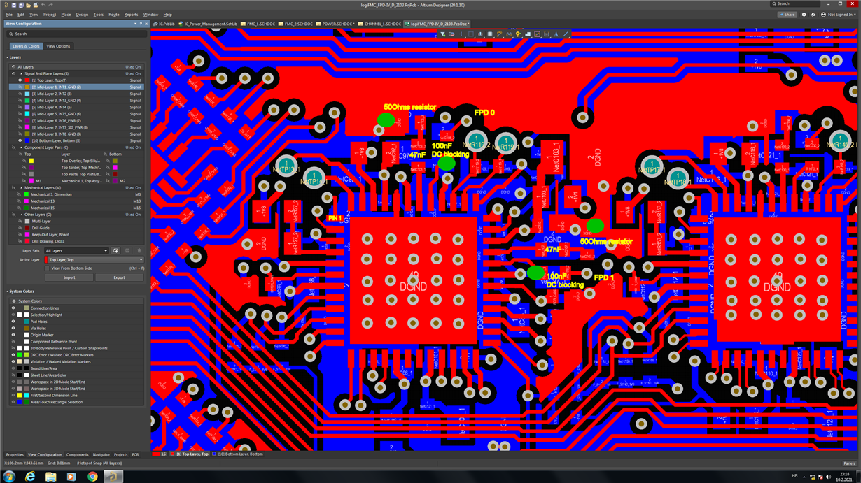
    Can you please put some labels on your picture above to where the FPD routing is? I can't really tell which way the chip is rotated based on this picture and the net labels don't give my info.

    Have you also checked the schematic components against the datasheet? i.e. power supply decoupling caps, ferrite beads?

    Best Regards,

    Casey 

  • Hi Casey,

    I put some labels. Hope it helps. Green ellipses are the points where I was connecting coaxial cable when I was trying direct cable connection to the deserializers. Understand that we should be using stitching vias (2 or 4 of them) at the points where FPD link PCB trace changes layers (FPD PCB trace is single-ended stripline routed on internal layers), but again, even without all that channel '1' looks OK, and discarding FPD PCB trace from the picture by direct cable connection does not solve the problem. I also attached a part of the schematics showing one out of 6 deserializers  The only power supply pins where we are measuring excessive noise are the pins 3 and 20. The other power supply pins are within tolerances. I tried adding a lot of additional capacitors (10u, 100n,, 10n) directly to these pins but that did not help. Wondering constantly if there is some register tweak that we could try...

    Regards

    Goran

  • Hello Goran,

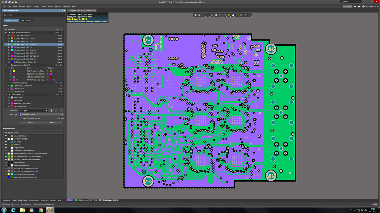
    What does the next layer down from the top look like especially under the high speed routing? Is it a solid ground plane? I don't see any obvious issues with the routing straight away, but it may take a more detailed level simulation analysis to see if there are any major SI differences between the total trace routing from chip to connector. 

    Anyways is this an issue you are only seeing on one system? Is it consistent across multiple? The MAP results actually don't look unreasonable. Sure there is less margin on port 0, but there is still sufficient margin that I would expect the link to work well. Are you getting errors or problems with LOCK in this system? 

    I would not recommend applying any register tweak. The driver/receiver is tuned to ensure performance of the link over PVT in a system which meets the SI specifications for the high speed channel. One thing you could do if you don't need the full CSI-2 BW for this application is to drop the link rate in half by setting 25Mbps back channel in register 0x58. That will drop the FC link rate to 2Gbps in synchronous mode and should give better sampling margin. That means the maximum CSI-2 rate on the 953 side also drops to 400Mbps/lane  

    Best Regards,

    Casey 

  • Hi Casey,

    I attached several more images of board's layout. We actually have a total of 4 solid GND planes. The first one is located directly under the TOP layer (Layers 1 and 2, TOPandGNDPlane.png, - check the layer list in the top left corner for the description of layers). FPD lines are routed as striplines in between two solid ground planes (INT2andGNDPlane.png and INT4andGNDPlane.png - only one plane is shown - the other is basically identical). We did SI simulation and found that impedance discontinuities are within +-10%. We are also about to perform TDR measurements on FPD lines to verify simulation results.

    Unfortunately, the issue can be observed across all the boards but it is not consistent. On one board, a channel that has a perfect MAP result may be totally unusable on the other board (MAP result doesn't even satisfy minimal requirements). That would suggest that there is something wrong with a way how boards are manufactured but we just can't see any obvious error. That's why I was hopping that you might have some ideas about what else, besides FPD link impedance, might be causing bad MAP results since that would give us some direction on where to look.

    Regards

    Goran

  • Hello Goran,

    It will take some time to look at this in detail. I will respond back early next week Monday or Tuesday 

    Best Regards,

    Casey 

  • OK, Thanks!.

    Regards

    Goran

  • Hello Goran,

    I can't see any obvious issue here in the layout that would cause a drastic difference in performance from one board to the next. But I do agree with your comment that it sounds like it could be a manufacturing issue. Have you tried reflowing one of the parts on the board which is not working well to see if the behavior changes?

    Best Regards,

    Casey

  • Hi Casey,

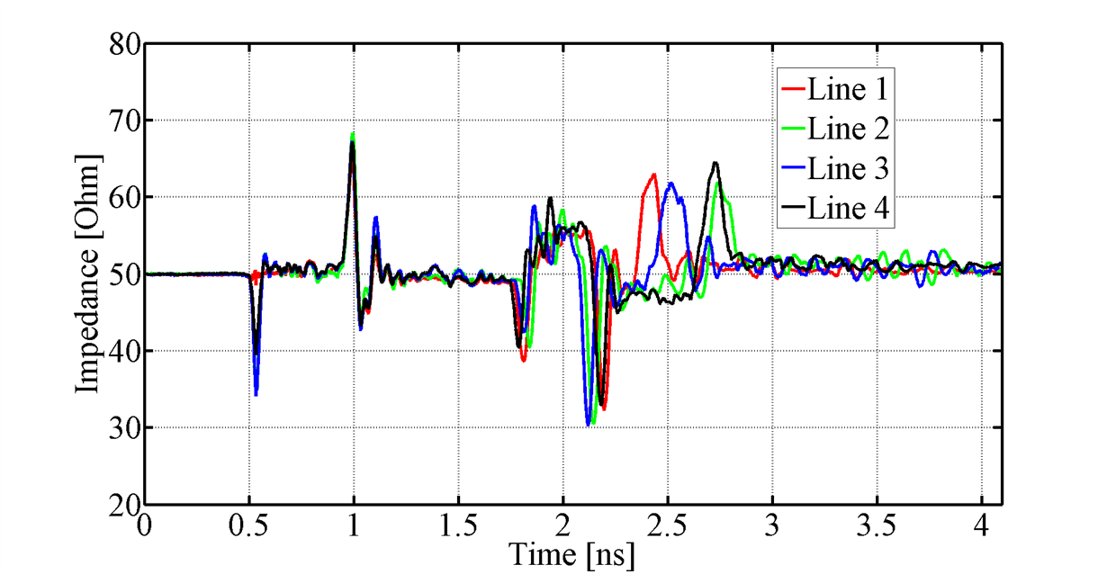
    Thanks for your answer. I did try to re-solder one of the deserializers (I removed it completely and then I solder it again) but  that did not help. Today we got TDR measurements of four FPD lines (attached). Lines were terminated with 50 ohms resistors. PCB connector starts at 2 ns. As you can see we have pretty big discontinuities at the input connector (impedance falls below 50 ohms) and at the VIA where signal is switching layers - impedance greater than 50 ohms (simulation results were much better). However, it looks that all four lines are equally "bad" so again, I would expect similar behavior on all the channels. Since it is not so, is it possible that the deserializer itself simply has more tolerance for FPD line imperfections on channel 1 than it has on channel 0 (Since channel 1 is OK in majority of the cases)? I am not implying here that the dserializer itself is responsible for the problem we are experiencing, just that there might be some asymmetry between channels.

    Regards

    G oran

  • Hello Goran,

    Yes there may be some asymmetry from channel to channel or device to device. I do not believe for this device that there is a general trend though that channel 0 performs any worse than channel 1. For reference, if you want to make a comparison you can purchase the 954 EVM from TI.com and see how it performs channel to channel and you ca even populate one of your devices on that PCB to see if you see the same phenomenon 

    Best Regards,

    Casey 

  • Hi Casey,

    Today I swapped position of two deserilizers (one had both good channels and the other had only one good channel). After that, the one with previously both good channels still performed well on both channels even at a different board position. The one with just one good channel performed well also on just one (the same) channel. TDR results may also be better than they look at first. The lab that did TDR measurements for us used step pulse with 25 ps rise time. According to 953 datasheet, typical forward channel rise time is 65 ps so the actual bandwidth should be narrower and discontinuities less pronounced. We are checking this right now in simulations...

    Regards

    Goran

  • Hello Goran,

    Is there any chance that the device is getting damaged on your board during testing? Are you using PoC here for the channel? What is the PoC voltage?

    Best Regards,

    Casey 

  • Hi Casey,

    No, I don't think that device is getting damaged. The PoC voltage is 12V maximum, and DC blocking capacitors are rated at 35V.

    Regards

    Goran

  • Hello Goran,

    Yes but the RIN pins are not rated for high voltage and during a transient (ex. turning on the PoC input with a very fast slew rate), the RIN pins may see higher transient voltage than expected, exceeding the abs max for the pins. It might be worth checking if the PoC power up slew rate is extremely high and what voltage is getting to the pins of the device at the time when the PoC is powered on/off 

    Best Regards,

    Casey 

  • Hi Casey,

    I measured what is happening at both P and N FPD pins when PoC power is turned on. When on -board power supply is used (normal use-case) there are no visible transients probably because power supply output ramps up slowly and monotonically. In some tests I removed on-board power and connected external power supply for providing power to the imagers. In that case there is a small transient (2.8V peak at P pin, and 2.3V peak at N pin) . During transient, voltage is above 2V for about 10 us and exceeds 2.75V maximum rating for a fraction of that time (At P pin only). Can't tell for sure if this could have damaged the chip, but even with on-board power supply and before I switched to external power deserializer's behavior was more or less the same.

    Regards

    Goran

  • Hello Goran,

    I'm not sure what additional support you are still looking for here. My recommendation would be to first clear up the issue with the power supply ripple ~80mVpp and also see if you can get the impedance continuity closer to 50 ohms along the channel including the connector region and then revisit this. 

    Also, did you ever post any snapshot of the schematic portion where you have PoC? Can you share that for review as well so we can verify the component selection?

    Best Regards,

    Casey 

  • Hi Goran,

    Just curious! Do you know how TDR lab performed the TDR measurement? In my opinion, the 95x has a slower rise time where you are trying to get the fast edge. If you do, then it is too fast for the device and will never see the impedance differences. If you are going slower than the specs of 65ps then it will mask out the mismatch. I would suggest you to try out at least 45ps to 65ps.

    Hope this helps. Let me know if you have further questions.

    Aaron