This thread has been locked.

If you have a related question, please click the "Ask a related question" button in the top right corner. The newly created question will be automatically linked to this question.

DP83620: About DP83620 chip CLK_OUT pin pull down the crystal output problem

Part Number: DP83620

Hi team,

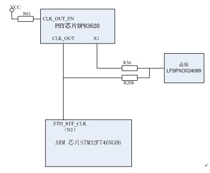
The crystal oscillator output on our product board is simultaneously connected to X1, clk_out of the DP83620 chip, ETH_REF_CLK (N2) of the ARM chip, clk_out_en is floating, R36 and R208 are 0R resistors, and the crystal oscillator uses CMOS-3.3V-15pf-25ppm, as shown in the figure below:

When the controller network is normal, the maximum amplitude of the 50M waveform measured by the crystal oscillator is 2.8V. When the network is abnormal, the maximum crystal oscillator output waveform is 1.8V.

(1) Connect clk_out_en directly to the ground, the crystal oscillator output waveform amplitude is up to 2.8V, and the network connection is normal;

(2) Floating clk_out_en, R36 and R208 are 0R resistors replaced by 22R resistors or 0.01uf capacitors, the crystal oscillator output waveform amplitude is maximum 2.8V, and the network connection is normal;

(3) The original circuit remains unchanged, the front end of the 24V-5V-3.3V circuit is changed to 5V for direct power supply, the crystal oscillator output waveform amplitude is up to 2.8V, the network connection is normal, and the power supply waveform is measured;

Ask the question:

(1) When the clk_out_en of the DP83620 chip is directly grounded and floating, what is the difference between the state of the CLK_OUT pin;

(2) Why can it be changed to 22R resistor or 0.01uf capacitor? Is it the impedance matching effect, or the direct current component, or the voltage is pulled down by too much load? What is the specific mechanism?

(3) The influence of the power supply on this part of the crystal oscillator circuit

BR

Brandon.

  • Hi Brandon

    If left floating it could be in a tri state at reset so I'd recommend grounding the pin just to ensure you know the correct state of that pin

    Can you explain when exactly these abnormal and normal behaviors happen on the crystal? Have you tried testing it in the crystal recommendation we have explained in our datasheet?

    Thanks

    Cecilia

  • HI Cecilia,thanks to your answer。

    These abnormal behaviors occur when the power on, the crystal oscillator output waveform amplitude is pulled to 1.8V, analysis PHY can not detect the clock signal, also can not work. Excuse me, CLK_ Out in CLK_ out_ Is the state of en floating and pulling down Hi-Z or low resistance to ground?

    Thanks

    Mazhou

  • Hi Cecilia,

    Mazhou is my customer engineer, hope you could help him solve the problem we met now.

    BR

    Brandon.

  • Hi Brandon

    I am not understanding the question can you please clarify what you mean by: Excuse me, CLK_ Out in CLK_ out_ Is the state of en floating and pulling down Hi-Z or low resistance to ground?

    If the PHY is left floating it could be in an unknown state so to be safe and ensure that it is in the correct mode I suggest pulling to GND. 

  • Hi Cecilia,

    (1)the datasheet paga 10 say  "If the default option is required, then there is no need for external pull-up or pull down resistors. Since these pins may have alternate functions after reset is deasserted, they should not be connected directly to VCC or GND."and  CLK_ out_EN is PD(pull down) ;you say "If the PHY is left floating it could be in an unknown state"; it is  Conflicting.

    (2)when CLK_ out_ EN Is the state of  floating or pulling down,what's the different pin state of CLK_ Out ?

    (3)Is this application correct,What is the effect of connecting crystal oscillator output to phy CLK_ out?

    look forward to your reply。

     Mazhou