This thread has been locked.

If you have a related question, please click the "Ask a related question" button in the top right corner. The newly created question will be automatically linked to this question.

SN65DP159: Is it possible to perform the bus clear operation defined in the I2C standard with the DDC?

Part Number: SN65DP159

When an HDMI 2.0 compatible Sink device is connected, the Soure device periodically reads the SCDC register according to the standard, but unfortunately if the Source device is turned off or the cable is disconnected in the ACK state, The Sink device keeps the SDA low. The I2C standard stipulates that the master device performs a BUS Clear operation when such a situation occurs. Is it possible to generate these 9 dummy clocks?

I am trying to implement this function by GPIO control, but the signal is different between SCL_SRC / SDA_SRC and SCL_SNK / SDA_SNK and I cannot implement it.
Does the "ACTIVE DDC BLOCK" depicted in the functional block diagram of the data sheet implement functions other than level conversion?


  • Hi,

    The active DDC block does more than the level shifting between the source and the sink. It also implements clock stretching which will hold the SCL_SRC low on the Source side while waiting for a response from the Sink.

    If the DP159 locks up during the BUS Clear operation, you have to toggle the OE pin to reset the Dp159.

    Thanks

    David 

  • Thank you for answering

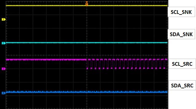
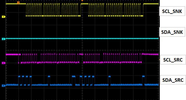
    But I don't understand how DP159 works. Our circuit connects the output of the Xilinx HDMI TX IP to the DP159. Experimentally, I fixed SDA_SNK to the LOW level while connecting to the monitor with an HDMI cable and checked the status of DDC. As a result, the waveform shown below was obtained. Since the BUS Clear function is implemented in Xilinx IP, SCL_SRC is toggled when SDA_SRC is LOW, but this signal is not transmitted to SCL_SNK. In addition, SDA_SNK may open SDA_SRC even though it is LOW. ・ As far as I read the data sheet, it seems that there is nothing, but can I set the bypass to just shift the level of the DDC? ・ Are there any precautions for the SCL_SRC signal required to perform BUS Clear? ・ I think that the PD_EN operation of the I2C register has the same effect as toggling the OE pin, but is it necessary to toggle the OE pin?

  • Hi,

    The DP159 implements clock stretching on its DDC bus, and there is no way to bypass the DP159 clock stretching and just use the level shifting function. If you need just the level shifting function, then you would need an external level shifter.

    You can use the PD_EN to reset the DP159 as well.

    Thanks

    David

  • Thank you for answering

     One more thing I would like to confirm, is it correct to understand that DP159 cannot support SCDC read requests?

  • Hi,

    The DP150 will pass through the SCDC read request.

    Thanks
    David