This thread has been locked.

If you have a related question, please click the "Ask a related question" button in the top right corner. The newly created question will be automatically linked to this question.

TMDS181: Wrong output waveforms

Part Number: TMDS181


Hi,

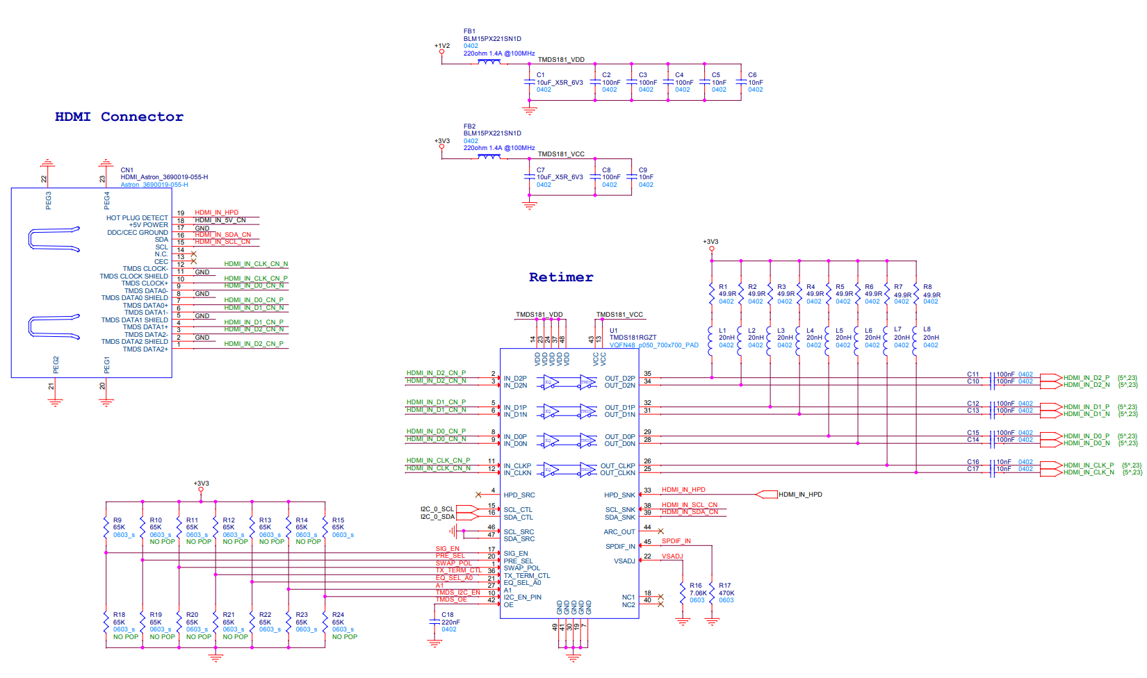
I'm encountering some troubles with the TMDS181.

I use this device in order to create an HDMI input which is connected to a FPGA (Zynq US+)

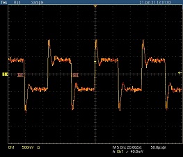
The output waveforms are not correct, I have some kind of de-emphasis, see below:

I'm using I2C configuration, I didn't modified the default values.

I also tried pin strapping mode, it didn't changed anything.

I always have the same issue whatever the bitrate I use.

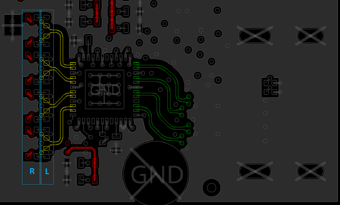
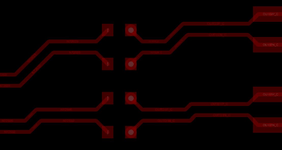
Here's the schematic:

Thanks,

Pierre.

  • Pierre

    Where do you measure the output signal? Is the FPGA still connected to the output when you measured the waveform?

    Can you please remove the inductors on the external 50ohm termination?

    Thanks

    David

  • I did the measurement right after the capacitors.

    Yes the FPGA was connected and configured when I did the measurements.

    I've already tried to remove the inductors, it's quite better but still not good.

  • Pierre

    Is it possible to remove the capacitors and repeat the measurement?

    Thanks

    David

  • Hi David,

    I removed the capacitors and did the measurement again, it's worst.

    That means it don't depend on the load.

    In I2C mode, do I need to configure something?

    Pierre.

  • Pierre

    What is the data rate you are running? In I2C mode, you need to configure the TX_TERM_CTL.

    • Data rate (DR) > 3.4 Gbps – 75 to 150 Ω differential near end termination
    • 2 Gbps > DR < 3.4 Gbps – 150 to 300 Ω differential near end termination
    • DR < 2 Gbps – no termination

    Please also check HDMI_TWPST1[1:0], by default, it should be set to 0dB de-emphasis (0x00).

    Can I also take a look at your layout?

    Thanks

    David

  • I tried different bitrates, I always have the problem. I'm currently running at 1.485 Gbps.

    HDMI_TWPST1 is at 0.

    Here are the registers: 

         0  1  2  3  4  5  6  7  8  9  a  b  c  d  e  f
    00: 54 4d 44 53 31 38 31 20 01 02 b1 18 00 00 00 0f 
    10: 00 00 00 00 00 00 00 e0 80 00 d0 04 00 00 00 00

    Below is the layout:


  • Pierre

    You had the termination set to 0x11, which is 75-150ohm. This should be set when the data rate is > 3.4G.

    For data rate of 1.485G, the termination should be set to 0x00, which is No Termination.

    On the layout

    1. Do you have solid reference ground underneath the high speed signal lanes?

    2. I would remove the inductor, and move the 50ohm termination resistor to the backside of the board and via directly to the capacitor pad to minimize the stub as much as possible. Below is an example

    Top layer (cap)

    Bottom layer (pull-up resistor plus the 3.3V power plane)

    Are you also seeing this issue on both the clock and the data output?

    Thanks

    David