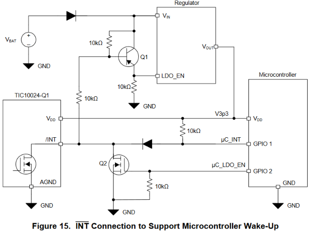
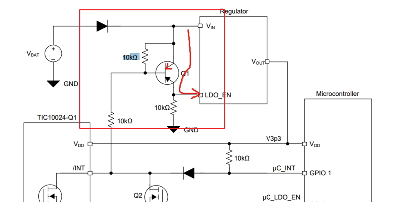
Part Number: TIC10024-Q1
Hi
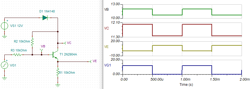
1. Whether the shutdown of logic electrical VDD will affect the INT interrupt
2. Can VDD be turned off at low power consumption
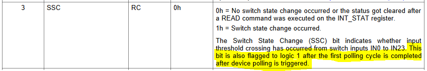
3. When configured to Polling mode, input interrupt is opened, INT will always be low, what is the reason for this phenomenon?
4. Can you provide routine
thanks!