This thread has been locked.

If you have a related question, please click the "Ask a related question" button in the top right corner. The newly created question will be automatically linked to this question.

TPS65987D: TPS65987D

Part Number: TPS65987D
Other Parts Discussed in Thread: TPS55288, TPS25750, TPS65987

Hello,

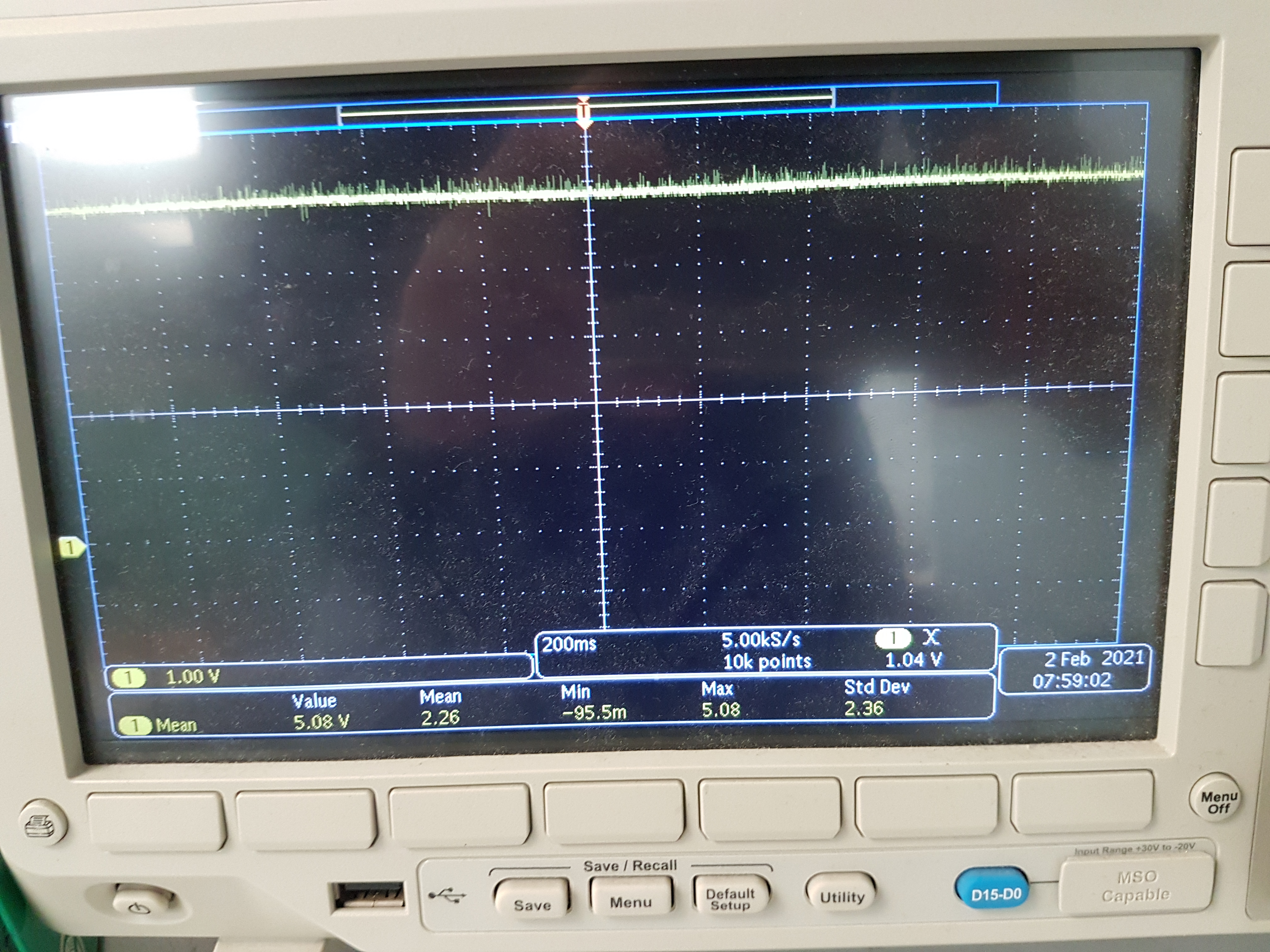
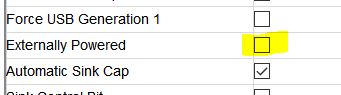
At this moment, I am debugging my own design PCBA that includes TPS65987D and TPS55288. I set the TPS65987D to be DFP, source and 4 PDOs source capabilities using application customization tool. The TPS65987D can initialize the TPS55288 and set it as 5V by I2C3 port. In addition, the VBUS can also output 5V and one of the CC pin is pulled to 1.6V from 5V once the USB type C loading is inserted. However, the TPS65987D never send out its source capabilities to the loading. Do I set anything wrong in the application customization tool? My application customization project file is also attached here for reference. Would you help to check anything I missed in the setting? Thank you!!

Thank you for your help!

Best regards!

Alanproject3.pjt

  • Hi Alan,

    If you are just using the PD controller for DFP, sourcing and do not require DP or Alternate Mode capability, I recommend taking a look at the TPS25750.

    For your issue though could you double checking your flash configurations and VIN_3V3 to make sure it's powered on. Also, once you have flashed the configuration project on your board you will have to power cycle the board so that the PD controller can load the new patch from the Flash.

    I will also take a look at the project configurations and provide feedback by the end of the week.

    Thank you,

    Hari

  • Dear Hari,

    Thank you for your quick reply and it is really help. Thank you for your suggestion of TPS25750 however the TPS65987D will be implemented under DP mode and alternate mode.

    Besides, I have double checked the hardware external flash configuration and VIN_3V3. There is VIN_3V3 to supply the TPS65987D and it can outputs the LDO_3V3 to supply the external flash W25Q80DVSNIG. Please see my schematics in the attachment for the reference. After powering the TPS65987D, there are some communication signals, which are shown on another jpg attachment (In that jpg, the CRO yellow line is SPI_CLK. Blue line is SPI_MISO. Red line is SPI_SS), over the SPI pins. Also, each time I update the external flash, I power down and then power up the PCBA to let the PD controller have power cycle to load the new patch from the external flash.

    In addition, for making sure the patch is loaded into the PD controller, I also change the logic level of one of the unused GPIO by "application customization tool" and that GPIO can toggle as what I desire after download and reboot.

    The above is what I have done before.

    Thank you very much!

    Best regards!

    Alan

  • Hi Alan,

    I will review the schematic and provide feedback by Friday. I would also recommend double checking ADCIN pins to make sure they are configured properly to have the PD controller program the configurations from Flash.

    Thank you,

    Hari

  • Dear Hari,

    The ADCIN1 just connected to the ground by 100K and SPI_MISO is pulled up by 3K3. The device's behavior should be safe configuration after booting.

    Best regards!

    Alan

  • Hi Alan,

    The schematic looks fine to me, I think it may be a programming issue. How are you flashing your board? If you have a new Flash IC on your board, you will have to make sure that you are programming the full flash image binary to it, however if you are only using the GUI, it may only be flashing the low region binary. If the Flash IC is new, it won't have the any region pointers in there that are needed for the PD controller to pull the configurations from which could be the reason you are not seeing the right functionality.

    Thank you,

    Hari

  • Dear Hari,

    Thank you for your reply and suggestion. First of all, I download the full image (Low region + High region) bin file using application customization tool and the Aardvark debugger. Two download methods have also been tried as below:

    1. Binary -> Flash from binary -> Select bin file -> OK -> After sometimes, the message "SPI Flash to Device successful" is shown -> Reset the power of my PCBA -> Plug the USB type C loading including 5.1K on CC -> No advertise from CC pin

    2. Binary -> Flash from current project -> Read current region offset (After reading, region 0 = 0x2000, region 1 = 0x6000) -> OK -> After sometimes, the message "SPI Flash to Device successful" is shown -> Reset the power of my PCBA -> Plug the USB type C loading including 5.1K on CC -> No advertise from CC pin

    I also read out and double check the contents from the external flash after re-flashing. There are region 0 and region 1 pointers located at 0x0000 and 0x1000 respectively. Please see the flash memory organization of my current setting as below:

    0x0000: Region 0 pointer

    0x1000: Region 1 pointer

    0x2000: Data setting or configuration (Region 0)

    0x3000: Firmware (Region 0)

    0x6000: Data setting or configuration (Region 1)

    0x7000: Firmware (Region 1)

    In addition, I debug the TPS65987D online as well and it can show me that there are 4 source capabilities PDOs, which I created in the application customization tool, in the register 0x32.

    That is my situation now.

    Besides, the bin file "TPS65987_88_F707_10_08.bin" is used as the firmware base image in my project. However, I found that its firmware image content (Its firmware is located at 0x1000) is different from that of the bin file "tps65987_evm_flash_image.bin" (Its firmware is located at 0x2000). Is it OK to use TPS65987_88_F707_10_08.bin as the firmware base image? Did you found anything wrong in my project file what is sent to you last week?

    Best regards!

    Alan

  • Hi Alan,

    From your description, I still suspect this may be a power related issue. The regions should not be too big of a deal as long as the project file is configured correctly for it. Since you were able to go to debug mode on your board and see the 4 source PDOs, then I think it may be a hardware issue. Could you please provide a PD log showing the communication between the 2 PD devices?

    Also, I see that you have connected VIN to PPHV, could you tell me where this VIN comes from and if it is capable of providing all of the voltages that you have configured in your Source PDOs? It might also be a good idea to scope the VBUS, PPHV, VIN_3V3 and CC pins to see how they behave at the time you connect the Type-C cable.

    Thank you,

    Hari

  • Dear Hari,

    Thank you for your reply and your help. Unfortunately, I don't have the PD log among those 2 PD devices since there is no communication on CC line at all. This is also my original issue.

    The VIN comes from TPS55288 and it is supposed to provide the voltage 5V, 9V, 15V, 20V to TPS65987D which is shown in my project file inside the attachment below. Also the schematic related to TPS55288 is displayed below.

    The Vout connects to the VIN of TPS65987D. The I2C3 of TPS65987D controls TPS55288. In addition, The VBUS waveform is shown below after plugging the PD loading device. There is some noise over the VBUS.

    The waveform of VIN_3V3 is 3.3V (Nothing special).

    CC1 is around 1.6V and CC2 is around 0.4V respectively.

    I think that the issue is not related to the power.

    Best regards!

    Alan

    2541.project3.pjt

  • Sorry, I made a mistake on posting the TPS55288 schematics on the above reply. Please check it here.

    Best regards!

    Alan

  • Hi Alan,

    Thank you for providing the schematic and the scope capture. For CC1 and CC2, are they constant at this value or toggling? I will look further into this to see if we can find the issue and provide some feedback later in the week. 

    I would also recommend getting an EVM to test on first with your project files so this way we can isolate the issue to the board.

    Thank you,

    Hari

  • Dear Hari,

    Thank you for your suggestion.

    The CC1 and CC2 never toggle.

    Besides, I have already ordered the TPS65987D EVM today. Hope it to help to solve the issue.

    Best regards!

    Alan

  • Dear Hari,

    The CC1 and CC2 keep at their constant voltage (1.6V) if it is set as DFP when PD loading plugging in. On the other hand, when I set it as DRP, CC1 and CC2 can toggle between 3.3V and 0V. However, when the PD loading plugging in, both of CC still cannot signal out the source capabilities. Should the TPD65987D send out the PD signal first (before anything happens) once it detects the 5.1K resistor on the CC pin?

    I have already ordered the TPS65987D EVM yesterday. Hopefully, it can help to solve the issue.

    Best regards!

    Alan

  • Hi Alan,

    Unfortunately, it is difficult to see what the issue could be without PD logs. We can see if you are able to reproduce this issue on the EVM so we can see if it may be a HW issue or something else. What device are you connecting your board to? Also, when you say PD loading plugging in, are you referring to when the two devices are connected?

    Thank you,

    Hari

  • Dear Hari,

    Thank you for checking my project file. At this moment, I think that I need to check with the EVM first but I am still waiting for my company to approve to buy the EVM.

    Best regards!

    Alan

  • Hi Alan,

    Yes I think once you receive the EVM it should help to see the different behavior. I have some suggestions on other settings you can try: 

    • In Port Control, could you check the Externally Powered field?


    • Also, in Port Configuration I noticed that you are have VCONN support, however I do not see that you have PPHV1 connected to a 5V source, is that correct? For VCONN support, the PD controller must be able to provide constant 5V, however on your schematic I don't think I saw this.

    Thank you,

    Hari

  • Dear Hari,

    Sorry for my late reply because of the Chinese new year holiday. My new EVM has been arrived and I will trouble shoot with it.

    For the "Externally powered" field, I will check it to see what happen.

    For the "VConn Supported" field, I should select "VCONN supported as DFP only", not "VCONN supported as DFP/UFP". It should be a mistake. However, in the hardware side, constant 5V has been already applied to the pin "PP_cable" for VCONN support. It seems that no need to provide 5V to PPHV1 for VCONN. Am I correct?

    Best regards!

    Alan

  • Hi Alan,

    That's great to hear you received your board. Let me know if you are able to reproduce the issue. Also, yes that's correct if you have the PP_Cable connected to the 5V supply then that should be good, I only saw the label on the schematic so wasn't sure where it was going.

    Thank you,

    Hari

  • Dear Hari,

    After testing with TPS65987D EVM, I think that the root cause of my issue has been found and now my hardware can communicate to the PD loading with changing the output VBUS from 5V to 20V. The root cause is that the VBUS1 pin must connect to the VBUS2 pin although I don't use VBUS1 for sink power. After I short the VBUS1 pin to VBUS2 pin, everything works fine.

    Lastly, thank you for your supply!

    Best regards!

    Alan

  • Hi Alan,

    I am glad you were able to resolve the issue and the EVM helped with you board as well! 

    Thank you,

    Hari