This thread has been locked.

If you have a related question, please click the "Ask a related question" button in the top right corner. The newly created question will be automatically linked to this question.

PCA9306: 200kohm requirement in case of Vref1=Vref2, pull up resistor placement

Part Number: PCA9306

Hello team,

My customer has reported that some PCA9306s seem to get damaged(resistance between SCL1(and/or SDA1) and GND is about hundreds ohm) and don't work.

Please see below left side for current PCA9306 connection. Customer uses same voltage to Vref1 and Vref2(not level translation).

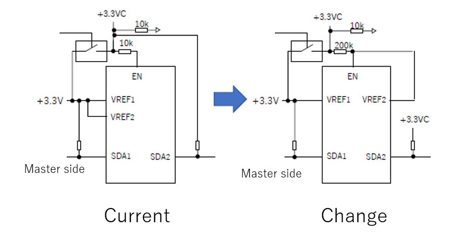
Do you think a cause of the damage is due to Vref2 connection not having 200kohm resistance?

Currently customer tries to modify the circuit to close to datasheet figure10.

Do you think above right side connection is better than current connection? or please let me know if there is other better connection.


By the way, pull up resistor for SCL1 and SDA1 is not on the PCA9306 board but on only I2C master side board. Should we place the resistor also in PCA9306 board?

Best regards,

  • Connecting EN to VREF2 works only when the requirements in section 9.2.1 of the datasheet are met. The proposed change does not conform to the circuit in figure 10. The current circuit should be kept.

    In the switch configuration in figure 10, the 200 kΩ resistor is not actually needed; its size does not matter.

    The exact placement of the pull-up resistors does not matter.

    Nothing in the schematics shown would explain the damage. I guess that the damage is caused by overvoltage.

  • Sato-san,

    Allow me to add some additional comments to the above. (Thanks for the response, Clemens!)

    As stated, neither of the configurations is expected to cause electrical damage to the device on its own, however, I have a suspicion that the +3.3VC switch may possibly be responsible for the damage being seen. This switch might possibly cause inductive kick/inrush onto the EN pin when enabled (especially if this is a tactile switch), and this could cause overvoltage on the EN pin, which would lead to damage. Please check to see if this is possibly the case.

    When VREF1 and VREF2 are shorted together as shown here, then you can implement this device without a resistor in place. However, even if VREF1 = VREF2, when these are controlled by different rails and therefore have a possibility of starting up at different times (i.e. not always being identical voltage), then a resistor would be needed.

    The proposed change would likely not damage the device, as this is actually similar to the layout shown in Figure 11 of the PCA9306 datasheet. The issue is that you would not satisfy the condition "Vcc2 >= Vref1 + 0.7 V" since the voltages are the same. This would result in increased propagation delays and altered performance characteristics, as a falling edge would need to be driven lower than usual to get it to pass along to the other side of the device.

    Please add a comment if you have any further questions!

    Best,

    Danny