This thread has been locked.

If you have a related question, please click the "Ask a related question" button in the top right corner. The newly created question will be automatically linked to this question.

DS90UB953-Q1: Input source check (MIPI) register

Part Number: DS90UB953-Q1
Other Parts Discussed in Thread: ALP

Hi Team,

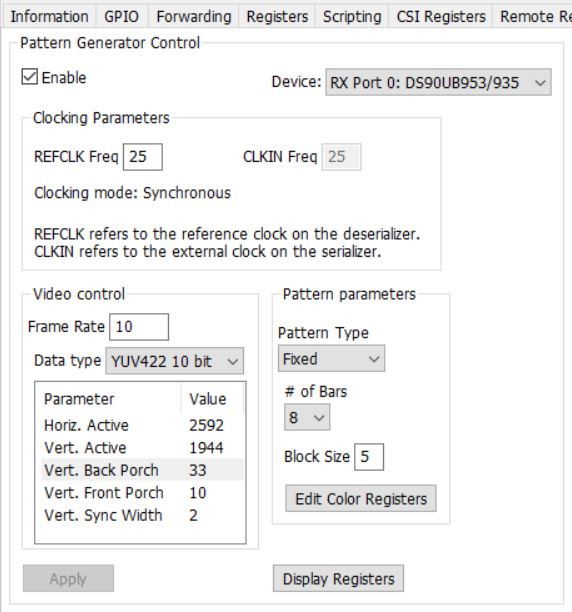
My customer is using 953+954 now. We check they could link each other. But it could transmit the data through FPD-link.

1. Do we have register that indicate the 953 get the correct MIPI data or not?

2. Are 953 + 954 auto transmit? I mean we dont need to modify the specific register to turn on the FPD-link port, right?

Roy  

  • Hi Roy, 

    On the 954 side, you will need to enable the CSI transmitter in order to turn on the output port. Please see section 5.2 

    THanks

    sally 

  • Hi Sally,

    We check the section 5.2, but it still couldnt work. Could you help let us know whether we have another register need to modify?

    Our design is coax, synchronize mode(954->953) thank you

    953

    [REGISTERS]
    Device = ALP Nano 1 - DS90UB953/953A/951, Connector 1
    Comments = ""
    Date = 02/08/2021
    Time = 16:25:53
    Reg = 0,0x0000,0x30
    Reg = 0,0x0001,0x00
    Reg = 0,0x0002,0x32
    Reg = 0,0x0003,0x48
    Reg = 0,0x0004,0x00
    Reg = 0,0x0005,0x03
    Reg = 0,0x0006,0x41
    Reg = 0,0x0007,0x28
    Reg = 0,0x0008,0xFE
    Reg = 0,0x0009,0x1E
    Reg = 0,0x000A,0x10
    Reg = 0,0x000B,0x7F
    Reg = 0,0x000C,0x7F
    Reg = 0,0x000D,0xF0
    Reg = 0,0x000E,0x0F
    Reg = 0,0x0010,0x00
    Reg = 0,0x0011,0x00
    Reg = 0,0x0013,0x00
    Reg = 0,0x0014,0x00
    Reg = 0,0x0015,0x20
    Reg = 0,0x0017,0x3C
    Reg = 0,0x0018,0x80
    Reg = 0,0x0019,0x62
    Reg = 0,0x001A,0x62
    Reg = 0,0x001B,0x62
    Reg = 0,0x001C,0x00
    Reg = 0,0x001D,0x00
    Reg = 0,0x001E,0x00
    Reg = 0,0x0020,0x00
    Reg = 0,0x0021,0x00
    Reg = 0,0x0022,0x00
    Reg = 0,0x0023,0x00
    Reg = 0,0x0024,0x00
    Reg = 0,0x0031,0x20
    Reg = 0,0x0032,0x09
    Reg = 0,0x0033,0x04
    Reg = 0,0x0035,0x10
    Reg = 0,0x0037,0x7A
    Reg = 0,0x0039,0x00
    Reg = 0,0x003A,0x00
    Reg = 0,0x003B,0x00
    Reg = 0,0x003C,0x00
    Reg = 0,0x003D,0x00
    Reg = 0,0x003E,0x00
    Reg = 0,0x003F,0x00
    Reg = 0,0x0040,0x00
    Reg = 0,0x0041,0x00
    Reg = 0,0x0042,0x00
    Reg = 0,0x0043,0x00
    Reg = 0,0x0044,0x00
    Reg = 0,0x0045,0x00
    Reg = 0,0x0046,0x00
    Reg = 0,0x0047,0x00
    Reg = 0,0x0048,0x00
    Reg = 0,0x0049,0x00
    Reg = 0,0x0050,0x20
    Reg = 0,0x0051,0xC0
    Reg = 0,0x0052,0x47
    Reg = 0,0x0053,0x00
    Reg = 0,0x0054,0x00
    Reg = 0,0x0055,0x42
    Reg = 0,0x0056,0x00
    Reg = 0,0x0057,0x00
    Reg = 0,0x0058,0x07
    Reg = 0,0x0059,0x07
    Reg = 0,0x005A,0x07
    Reg = 0,0x005C,0x00
    Reg = 0,0x005D,0x00
    Reg = 0,0x005E,0x00
    Reg = 0,0x005F,0x00
    Reg = 0,0x0060,0x00
    Reg = 0,0x0061,0x2B
    Reg = 0,0x0062,0x20
    Reg = 0,0x0063,0x0D
    Reg = 0,0x0064,0x03
    Reg = 0,0x00B0,0x04
    Reg = 0,0x00B1,0x4A
    Reg = 0,0x00B2,0x3F
    Reg = 0,0x00F0,0x5F
    Reg = 0,0x00F1,0x55
    Reg = 0,0x00F2,0x42
    Reg = 0,0x00F3,0x39
    Reg = 0,0x00F4,0x35
    Reg = 0,0x00F5,0x33

    954

    [REGISTERS]
    Device = ALP Nano 1 - DS90UB954, Connector 1
    Comments = ""
    Date = 02/08/2021
    Time = 16:20:08
    Reg = 0,0x0000,0x7A
    Reg = 0,0x0001,0x00
    Reg = 0,0x0002,0x1E
    Reg = 0,0x0003,0x20
    Reg = 0,0x0004,0xDF
    Reg = 0,0x0005,0x01
    Reg = 0,0x0006,0x00
    Reg = 0,0x0007,0xFE
    Reg = 0,0x0008,0x1C
    Reg = 0,0x0009,0x10
    Reg = 0,0x000A,0x7A
    Reg = 0,0x000B,0x7A
    Reg = 0,0x000C,0x83
    Reg = 0,0x000D,0xB9
    Reg = 0,0x000E,0x00
    Reg = 0,0x000F,0x7F
    Reg = 0,0x0010,0x00
    Reg = 0,0x0011,0x00
    Reg = 0,0x0012,0x00
    Reg = 0,0x0013,0x00
    Reg = 0,0x0014,0x00
    Reg = 0,0x0015,0x00
    Reg = 0,0x0016,0x00
    Reg = 0,0x0017,0x00
    Reg = 0,0x0018,0x00
    Reg = 0,0x0019,0x00
    Reg = 0,0x001A,0x00
    Reg = 0,0x001B,0x00
    Reg = 0,0x001C,0x00
    Reg = 0,0x001D,0x00
    Reg = 0,0x001E,0x04
    Reg = 0,0x001F,0x02
    Reg = 0,0x0020,0x20
    Reg = 0,0x0021,0x01
    Reg = 0,0x0022,0x00
    Reg = 0,0x0023,0x00
    Reg = 0,0x0024,0x00
    Reg = 0,0x0025,0x00
    Reg = 0,0x0026,0x00
    Reg = 0,0x0027,0x00
    Reg = 0,0x0028,0x00
    Reg = 0,0x0029,0x00
    Reg = 0,0x002A,0x00
    Reg = 0,0x002B,0x00
    Reg = 0,0x002C,0x00
    Reg = 0,0x002D,0x00
    Reg = 0,0x002E,0x00
    Reg = 0,0x002F,0x00
    Reg = 0,0x0030,0x00
    Reg = 0,0x0031,0x00
    Reg = 0,0x0032,0x00
    Reg = 0,0x0033,0x03
    Reg = 0,0x0034,0x40
    Reg = 0,0x0035,0x00
    Reg = 0,0x0036,0x00
    Reg = 0,0x0037,0x03
    Reg = 0,0x0038,0x00
    Reg = 0,0x0039,0x00
    Reg = 0,0x003A,0x00
    Reg = 0,0x003B,0x01
    Reg = 0,0x003C,0x14
    Reg = 0,0x003D,0x6F
    Reg = 0,0x003E,0x00
    Reg = 0,0x003F,0x40
    Reg = 0,0x0040,0x00
    Reg = 0,0x0041,0xA7
    Reg = 0,0x0042,0x71
    Reg = 0,0x0043,0x01
    Reg = 0,0x0044,0x00
    Reg = 0,0x0045,0x00
    Reg = 0,0x0046,0x00
    Reg = 0,0x0047,0x00
    Reg = 0,0x0048,0x00
    Reg = 0,0x0049,0x00
    Reg = 0,0x004A,0x00
    Reg = 0,0x004B,0x12
    Reg = 0,0x004C,0x01
    Reg = 0,0x004D,0x13
    Reg = 0,0x004E,0x5D
    Reg = 0,0x004F,0x64
    Reg = 0,0x0050,0x00
    Reg = 0,0x0051,0x00
    Reg = 0,0x0052,0x00
    Reg = 0,0x0053,0x03
    Reg = 0,0x0054,0x06
    Reg = 0,0x0055,0x00
    Reg = 0,0x0056,0x00
    Reg = 0,0x0057,0x00
    Reg = 0,0x0058,0xDE
    Reg = 0,0x0059,0x00
    Reg = 0,0x005A,0x00
    Reg = 0,0x005B,0x30
    Reg = 0,0x005C,0x00
    Reg = 0,0x005D,0x00
    Reg = 0,0x005E,0x00
    Reg = 0,0x005F,0x00
    Reg = 0,0x0060,0x00
    Reg = 0,0x0061,0x00
    Reg = 0,0x0062,0x00
    Reg = 0,0x0063,0x00
    Reg = 0,0x0064,0x00
    Reg = 0,0x0065,0x00
    Reg = 0,0x0066,0x00
    Reg = 0,0x0067,0x00
    Reg = 0,0x0068,0x00
    Reg = 0,0x0069,0x00
    Reg = 0,0x006A,0x00
    Reg = 0,0x006B,0x00
    Reg = 0,0x006C,0x00
    Reg = 0,0x006D,0x7C
    Reg = 0,0x006E,0x88
    Reg = 0,0x006F,0x88
    Reg = 0,0x0070,0x2B
    Reg = 0,0x0071,0x2C
    Reg = 0,0x0072,0xE4
    Reg = 0,0x0073,0x07
    Reg = 0,0x0074,0x98
    Reg = 0,0x0075,0x0D
    Reg = 0,0x0076,0x20
    Reg = 0,0x0077,0xC5
    Reg = 0,0x0078,0x00
    Reg = 0,0x0079,0x01
    Reg = 0,0x007A,0x0C
    Reg = 0,0x007B,0xFF
    Reg = 0,0x007C,0x20
    Reg = 0,0x007D,0x00
    Reg = 0,0x007E,0x00
    Reg = 0,0x007F,0x00
    Reg = 0,0x00A0,0x02
    Reg = 0,0x00A1,0x0F
    Reg = 0,0x00A2,0x00
    Reg = 0,0x00A3,0x00
    Reg = 0,0x00A4,0x08
    Reg = 0,0x00A5,0x17
    Reg = 0,0x00A7,0x00
    Reg = 0,0x00A8,0x00
    Reg = 0,0x00A9,0x00
    Reg = 0,0x00AA,0x00
    Reg = 0,0x00AB,0x00
    Reg = 0,0x00AC,0x00
    Reg = 0,0x00AD,0x00
    Reg = 0,0x00AE,0x00
    Reg = 0,0x00AF,0x00
    Reg = 0,0x00B0,0x08
    Reg = 0,0x00B1,0x14
    Reg = 0,0x00B2,0x3F
    Reg = 0,0x00B3,0x08
    Reg = 0,0x00B4,0x25
    Reg = 0,0x00B5,0x00
    Reg = 0,0x00B6,0x18
    Reg = 0,0x00B7,0x00
    Reg = 0,0x00B8,0xFC
    Reg = 0,0x00B9,0x33
    Reg = 0,0x00BA,0x83
    Reg = 0,0x00BB,0x74
    Reg = 0,0x00BC,0x80
    Reg = 0,0x00BD,0x00
    Reg = 0,0x00BE,0x00
    Reg = 0,0x00BF,0x00
    Reg = 0,0x00D0,0x00
    Reg = 0,0x00D2,0x94
    Reg = 0,0x00D3,0x02
    Reg = 0,0x00D4,0x60
    Reg = 0,0x00D5,0xF2
    Reg = 0,0x00D6,0x00
    Reg = 0,0x00D7,0x00
    Reg = 0,0x00D8,0x00
    Reg = 0,0x00D9,0x00
    Reg = 0,0x00DA,0x00
    Reg = 0,0x00DB,0x18
    Reg = 0,0x00DC,0x00
    Reg = 0,0x00DD,0x00
    Reg = 0,0x00DE,0x00
    Reg = 0,0x00DF,0x00
    Reg = 0,0x00F0,0x5F
    Reg = 0,0x00F1,0x55
    Reg = 0,0x00F2,0x42
    Reg = 0,0x00F3,0x39
    Reg = 0,0x00F4,0x35
    Reg = 0,0x00F5,0x34
    Reg = 0,0x00F8,0x00
    Reg = 0,0x00F9,0x00
    Reg = 0,0x00FA,0x00
    Reg = 0,0x00FB,0x00

    Roy

  • Hello Roy,

    From the registers it looks like the link is established and the correct timing parameters are detected at both the 953 and 954 sides. Your CSI-2 transmitter is enabled and the RX0 port is forwarded correctly to the output. However you are getting a buffer error on the 954 side register 0x4E as well as some CSI-2 errors which is strange. What is the CSI-2 lane rate on the 953 side? Also what is the REFCLK value attached to the 954?

    Best Regards,

    Casey 

  • Hello Casey,

    Thanks for information.

    May you share the register that you initially check for link and timing parameters?

    954 : 0x04 = 0xDF (PASS/LOCK ok, REFCLK is detected.) I think this is ok.

    954 : 0x35 = 0x00, Is this ok? 0x35[1] = 0 which means Input streams are not synchronized, but we set synchronous mode.

    954 : 0x22 = 0x00, Not synchronous. 

    954 : 0x4D = 0x13, ok

    954 : 0x51-0x54, is our data ok? 

    Reg = 0,0x0051,0x00
    Reg = 0,0x0052,0x00
    Reg = 0,0x0053,0x03
    Reg = 0,0x0054,0x06

    0x4E and 0x7A is showing that checksum is error, may you let me know the possible reason? REFCLK is not stable?

    What is the CSI-2 lane rate on the 953 side? Also what is the REFCLK value attached to the 954? I will check with customer.

    Roy

  • Hello Roy,

    954 register 0x54 seems to indicate that the CSI-2 errors are originating on the 953 side so please do check the 953 side CSI-2 lane rate and the 954 REFCLK value. All the other registers look ok as you say 

    Best Regards,

    Casey 

  • Hi Casey,

    The lane rate is about 750MHz and REFCLK = 24MHz. Our image sensor is OV(OS05A20).

    Do you have any idea?

    Roy 

  • Hi Roy,

    Looks like the sensor that you are using is 5M pixel image sensor. Do you know what is the resolution, frame rate, and data ID that your customer is using? It is probably that they are exceeding FPD3 bandwidth. The maximum bandwidth for 953-954 FPD is 3.84Gbps with a 24MHz ref clock.

    Aaron

  • Hi Aaron,

    We only use 1080p and frame rate is 30. But our  0x73 ~ 0x76 register couldnt detect the correct information.

    DO you have any idea?

    Roy

  • Hello Roy,

    The max lane rate at the 953 side is related to the REFCLK value at the 954 in synchronous mode. The max CSI-2 lane rate is REFCLK*32 for synchronous mode which means in this configuration the max lane rate is 24*32 = 768Mbps which would be a MIPI CSI-2 clock of 384MHz. 

    The provided CSI-2 source at 750MHz = 1500Mbps will not work in this configuration as the link will not have enough bandwidth.

    Best Regards,

    Casey 

  • Hello Casey,

    Thank you for your information. I will let customer to lower down the lane speed, but it would spend a little time.

    But we would like to use 953 internal pattern generation first to see whether display could show pattern normally or not. Please see below setup and result.

    Could you let me know if the pattern is abnormal, what is the most possible root cause? data type or parameter?

    Regards,

    Roy

  • Hello Roy,

    The ALP tab looks like it is set up correctly and this pattern should be low enough BW to work with the link. Is the customer hitting the "apply" button to make sure that the pattern registers are being programmed into the 953? The image you sent shows the incorrect resolution: 1031x577 instead of 2592x1944. The reason that it looks like there is a mix of many colors per bar is due to the color registers setup. I would recommend using the same byte value for PGEN_COLOR0 - PGEN_COLOR4 since the block size is 5 bytes for this data pattern 

    Best Regards,

    Casey