This thread has been locked.

If you have a related question, please click the "Ask a related question" button in the top right corner. The newly created question will be automatically linked to this question.

DP83TD510E: XI input

Genius 17335 points
Part Number: DP83TD510E

Hello,

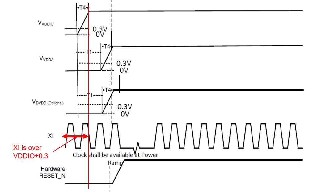
I have an question for XI input of DP83TD510E.
The absolute max voltage of XI input is defined as up to VDDIO+0.3V.
But in Figure 6-1 of the datasheet. XI is input before VDDIO ramp-up.
And there is a description, “Clock shall be available at Power Ramp”.
What does it mean?

Regards,
Oba

  • Hi Oba,

    VDDIO+0.3V is the max voltage that can be tolerated at XI pin. It is not the recommended voltage of operation, the recommended voltage of operation is VDDIO. Figure 6.1 indicates the sequencing of clock input and power ramp. Clock should be present before the power ramps up completely.

    -Regards

    Aniruddha

  • Hello Aniruddha,


    Thanks for your reply.
    In this figure, XI signal is present before VDDIO ramp up. It means XI is over VDDIO+0.3V. So I think this figure must be incorrect.


    And I think usually the oscillator IC generating XI signal is powered by the same voltage as VDDIO and it usually requires some start-up time after power-up.

    From the both reason, I think “Clock should be present before the power ramps up completely” is not reasonable request.


    Regards,
    Oba

  • Hi Oba,

    Should an external oscillator IC generate the XI signal, this clock shall also be powered externally. This external supply to power the clock should be enabled such that the clock is running before the PHY is powered on. "The absolute max voltage of XI input is defined as up to VDDIO+0.3V" refers to the amplitude of the clock signal itself. 

    What is the delay between clock start time and supply ramp? As long as clock is active before all supplies ramp, using VDDIO to power the oscillator IC should be ok.

    Thank you,

    Nikhil