This thread has been locked.

If you have a related question, please click the "Ask a related question" button in the top right corner. The newly created question will be automatically linked to this question.

SN65LV1224B: What is a state of Ri+/- when power supply does not supply?

Part Number: SN65LV1224B
Other Parts Discussed in Thread: SN65LV1023A

Hello Experts,

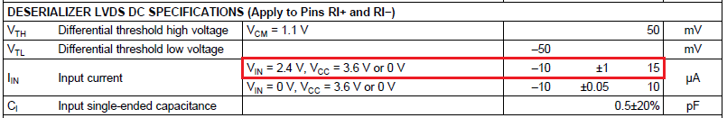
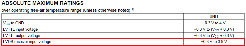
My customer is evaluating SN65LV1023A/SN65LV1224B configuration. Customer was adopted DS92LV1021A/1212A before, but he has changed to SN65LV1023A/SN65LV1224B due to EOL of DS92LV1021A/1212A. Are there any leakage current path from Ri+/i to Vcc-pin?
[customer use case]
Customer is using below configuration and these devices mounted on a different board.
<SN65LV1023A: Power supply is applied> ===> <SN65LV1224B: Power supply is not applied>

Customer mentioned that power supply rail of SN65LV1224B showed about 0.3V at the above configuration, but DS92LV1021A/1212A pair never show this phenomenon. Would you please answer it?

Best Regards,
Fujiwara

  • Hi Fujiwara-san,

    Please note that SN65LV1023A/1224B pair is not exactly the same as DS90LV1021A/1212A pair. Customer should reference this application note for migrating between the two: https://www.ti.com/lit/an/slla435/slla435.pdf 

    Since they're seeing 0.3V now when they weren't before then yes, it looks like there's a leakage current path from Ri+/- to Vcc (likely due to a protection diode).

    Regards,

    I.K. 

  • Hi I.K-san,

    I am supporting Japanese customers with Fujiwara-san.
    The datasheet shows the following so I believe we should measure input current in this case.
    Is my understanding correct?


    In addition, Is it possible for you to confirm if there is a leakage current path from LVDS receiver input to VCC?


    Best Regards,
    Yaita

  • I found the following with the application note you attached.


    So, I believe the following red part in SN65LV1224B datasheet is typo.
    Is my understanding correct?


    Best Regards,
    Yaita

  • Hi Yaita-san,

    No, that Input Current in the application note is referring to the LVCMOS/LVTTL input current. 

    I will check with design to confirm leakage current paths and will get back to you soon.

    Regards,

    I.K. 

  • Hi I.K.-san,

    >No, that Input Current in the application note is referring to the LVCMOS/LVTTL input current. 
    Is it true? I have thought it refers serial data input because SN65LV1224B has an on-chip fail-safe circuit that drives the serial input.
    I appreciate for your kind support and will wait for your feedback.

    Best Regards,
    Yaita

  • Hi Yaita-san,

    Good point. Depending on how the failsafe biasing is generated internally, it may or may not introduce additional leakage from I/O pins to VCC. 

    Design is looking at this but needs more information. Can the customer measure the leakage current that is sunk through LVDS input pins at the following 2 cases?

    • Un-power LV1224B with VCC floating
    • Connect VCC of LV1224B to ground

    Regards,

    I.K.