This thread has been locked.

If you have a related question, please click the "Ask a related question" button in the top right corner. The newly created question will be automatically linked to this question.

TUSB4020BI: Downstream port failures and will not connect to devices

Part Number: TUSB4020BI

Hi,

We are seeing high field failure rates on a board that uses the TUSB4020BI. Hoping you can help us understand what is going on.

Background:

This is a rugged field (highly custom) application where many small data recorders (nodes) are brought into a central location to dump their data. This central location is typically a trailer of some sort that is somewhat environmentally  protected. The nodes are loaded into racks to download data. The racks use several PCBAs, each with a TUSB4020BI to communicate to two nodes. So nodes are constantly being inserted and removed from the racks. The node is self powered so the hub TUSB4020BI is not doing any power control to the attached nodes, only high speed USB communications.

Failures:

We have started to see many boards that were previously working OK to suddenly stop connecting to a node as it is inserted. So far it has only been one of the two downstream ports (but can be either one) and the other port remains unaffected and working normally. SW or hard (power) reset does not recover the port once it fails. A failed board can be moved to a different location and the failure follows the board, so doesn't seem to be an issue with the Linux PC and main hub it is connected to. These boards do have a EEPROM for custom info but it seems to be OK. We have tried reprogramming the EEPROM, but this still does not fix the failure.

Debugging:

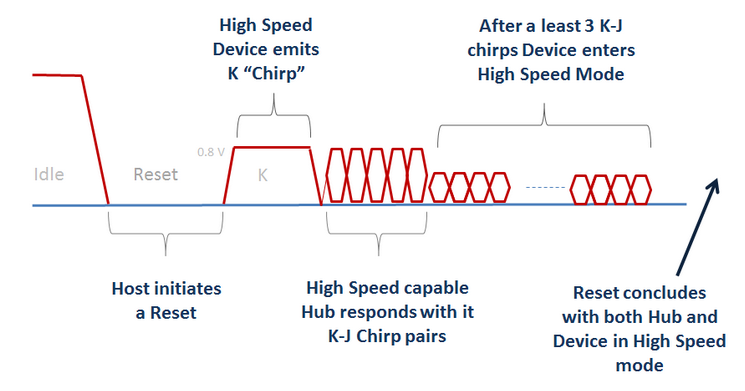
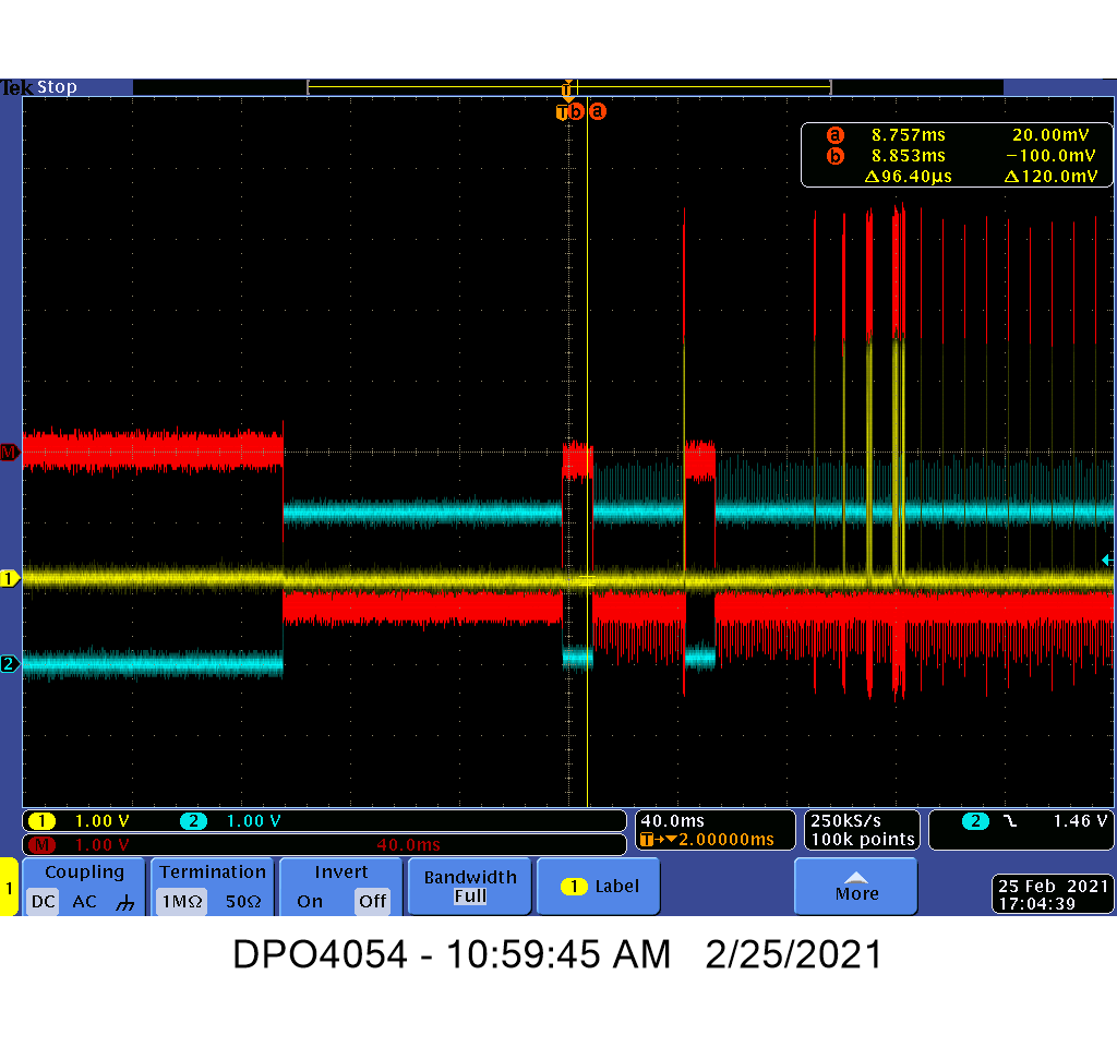
The failure is during the high speed device detection and speed negotiating phase. Testing on a Windows 10 PC reports a "Device Reset Error". I have looked at the signals on DP and DM with a scope and also connected a USB protocol analyzer to debug. This is what the typical high speed detection should look like:

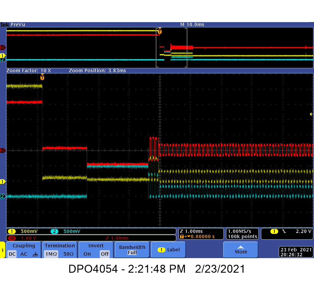
And this is what I see on working ports.

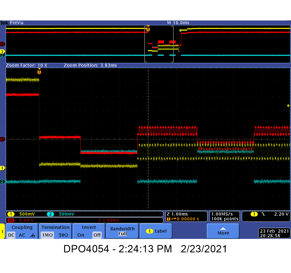
On a failed port I see:

1) The initial IDLE state with the device pulling DP high and DM is low. This is OK

2) The TUSB4020BI hub then drives DP low with DM still low to start a reset. This is OK

3) Our HS device then responds with a K chirp of about 2mS. Device drives DP low and  DM high, this is OK

4) The TUSB4020BI hub should then respond with K-J chirps on both DP and DM. This is where the failure appears to be. I only see the host K-J chirps on DP. DM is silent. It is almost as if the TUSB4020BI cannot drive the DM signal. The DP drive output seems to work OK.

We do have a ESD protection device on DP/DM (TPD2E2U06DRLR) but I removed it just in case it was the problem. Did not help and still have the failure. Nothing else is connected to DP/DM so it seems to be a failure in the TUSB4020BI DM output.

Any help would be appreciated.What failure modes could do this? Is it possibly ESD damage? How could we confirm this?

Just FYI, we inherited this board from another company. I found another thread on E2E from that company about other issues with this same board and TUSB4020BI. It can be found at the following link for more background info if helpful.

https://e2e.ti.com/support/interface/f/138/t/778963?TUSB4020BI-Downstream-port-s-become-unresponsive

Thanks,

Paul

  • Attached is the picture I thought was inserted in the the original post.

  • This is a scope capture of a "good' connection on my HW. Yellow = DP, Blue = DM and Red is the differential DP-DM. Note the good K-J chirps after the long device K chirp.

    And this is a failed connection. Note the lack of K-J chirps on the blue DM signal after the long device K chirp. DP K-J chirps look OK.

  • Hi Paul,

    The DM line looks damaged.  Can you try connecting a low speed device to the port (USB mouse) and capture what happens on the bus?  Also can you ohm the DM line to ground on a good port and on a bad port - without any downstream devices connected.

    Regards,

    JMMN

  • Hi JMMN,

    Thanks for the quick response. I connected a Low Speed (LS) Mouse and it connects and works on both good and "bad" downstream (DS) ports. But there are obvious differences.

    Here is a LS mouse connection on a good DS port. Again Yellow = DP, Blue = DM and Red is the differential DP-DM. On mouse connect (first transition) the mouse pulls DM high to signal a LS device. DM goes to about 3.3V here. Hub then drives DP/DM low to start a reset and proceeds form there to connect and enumerate OK. Both the DP and DM signals can drive to full 3.3V.

    Here is the same connection on the "bad" DS port. The signalling and timing look the same, but note that the DM signal can only drive to about 2.3V instead of 3.3V. So definitely looks like extra loading on the bad port DM line. But I guess it is still good enough for the LS logic to work and allows the mouse to operate at LS on the bad port.

    I also measured the the DP and DM resistance to ground as follows on two PCBAs, both with one good port and one bad port. DM lines on the bad ports are definitely lower than the good ports. Readings that look different to me are highlighted in yellow.

    To summarize:

    1) Low Speed device works on both good an bad ports but DM voltage levels on the bad port are low and seem to have extra loading on them.

    2) High speed device will not connect on bad port. The extra DM line loading seems to be too much for HS to work.

    3) Resistance readings on the DM line of bad ports are low.

    So question now is what could cause this? And how to prevent it in the field?

    Thanks,

    Paul

  • JMMN,

    one other probably unrelated item, but never hurts to double check. I noticed that the original designer left the TEST pin not connected so it is floating. In going through the TUSB4020BI datasheet and check lists, I noted that it should be pulled to ground. Will this cause a problem or in any way related to this issue?

    Thanks,

    Paul

  • Hi Paul,

    Yes, the TEST should be pulled to ground, but there is an internal pulldown on it and if the hub was entering test mode, the entire hub would not be functional.

    It is unusual to see port damage across multiple units in the field unless there is a common denominator like a bad cable or device that is causing electrical over stress events.  For example a frayed cable that is occasionally shorting power to the DM line,  Is there anything in common that got attached to all the bad units?

    Regards,

    JMMN

  • Hi JMMN,

    This is a very unique application. On the DS port side there aren't any USB cables or connectors involved. It is all mechanical. On the data recorder node there are just 4 metal pads on the outside of the enclosure that when placed in the rack they just mate to mechanical spring clips that are mounted directly on the PCBA with the hub chip. Think old style 900MHz cordless phones that are placed in the charging cradle when not in use. So no other USB devices could ever be attached, just nodes. Now they are inserted and removed quiet frequently. The four pads are Gnd, V+ (for charging the internal node battery), DP and DM.

    So the difference with a standard USB application would be that we have no back shell shield that mates first as you have when you plug a USB cable in that is connect to a chassis ground. Also as the design currently is, we cannot guarantee what signal makes connection first when inserting a node. We have looked at ways to make sure ground mates first but haven't worked that out.

    But having said all that, this has been in production for two years with hundreds of units in the field. We have seen some isolated issues in the past but are now suddenly seeing a sharp increase. But it is in a dessert  & dry environment where ESD could bemore of a problem. But with the ESD protection of the hub chip itself and the added TI TPD2E2U06DRLR ESD protection IC, we assumed it would still be OK.

    Any idea what magnitude of an ESD or over voltage event would be required to cause this type of damage? Assuming you concur that the DM pin has been damaged this way?

    Thanks,

    Paul

  • JMMN - should also note that the way the node is designed, it's internal USB device controller (a FTDI FT232HL) is not powered up when the node is inserted. The nodes first detects the presence of the external V+ then after a delay to allow any bouncing to die out, it then turns on the FTDI IC to start the USB connection to the HUB.

    The node's USB will be powered and communicating via USB when it can be suddenly removed from rack without warning. But that is no different than any other USB device.

    Paul

  • Hi Paul,

    Yes, it seems like some sort of EOS event, but it would be hard to determine what voltage or duration.  Can you check a few of the other bad units to see if the damage is consistent to DM on other boards?  That would indicate that there may be one particular node that is causing issues rather than it being randomly occurring.

    Regards,

    JMMN

  • Hi JMMN,

    I checked a third board and this one has a low ohm reading on the DP signal (about 10K instead of 20K as the other signals). So the issue does not seem to be confined to just the DM signal. Looks like the damage can randomly be either USB data line. Thus doubtful that a particular node caused this. That would be very low probability anyway the way the nodes are used in inserted into the racks.

    A bit more background on our system. This is how the USB is connected:

    PC (Linux OS)  <====> 24 port powered USB HUB <====> 24 two port cradles (TI HUB IC here) <=====> 2 nodes/cradle (x24, 48 total nodes per rack)

    The two port cradles are powered from a separate 12V supply but are enabled and powered up only when a good 5V is sensed from the 24 port powered hub via a standard USB cable to each cradle. On the cradle PCB we have two battery chargers (one for each connected node) that generates 8.6V charging voltage to the nodes when connected. The TI  TUSB4020BI then connects the USB to each of the two nodes.

    We apparently have the ability to turn off the 24 port powered USB HUB via SW from the Linux PC. This in turn would turn off the USB 5V to the cradles that would then also power down the cradle. Therefore there would not be any active voltages or signals on the cradle to node interface when nodes are inserted. The idea of powering down the USB hub and cradles while nodes are inserted/removed has been proposed.  I think this might help if the issue is with some over voltage or glitch/spike due to live power being applied as a node is inserted/removed. But I am not sure it would help or hurt if the issue is purely ESD discharge. I don't have a feel for if the PCB and ICs are more or less susceptible to ESD damage with power off. Thoughts?

    Also assuming it is ESD/EOS, can you or TI recommend additional ESD/EOS protection/filtering components or circuits to further harden the USB signals?

    Regards,

    Paul

  • Hi Paul,

    It is difficult to recommend protection without knowing what's causing the failure.  Have you removed any of the units from the boards?

    Please accept my friend request and let me know if you can send me a bad unit.

    Regards,

    JMMN

  • Hi JMMN,

    Sent you a private message.

    Paul

  • ok, responded there