This thread has been locked.

If you have a related question, please click the "Ask a related question" button in the top right corner. The newly created question will be automatically linked to this question.

SN75DP130: application

Part Number: SN75DP130

Hi team,

The following is the customer's question, please help to analyze

1. Video input board > FPGA > video output board (DP130) > 4K display, and the screen display is normal;

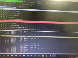
2. Video input board > FPGA > video output board (DP130) > analyzer report errors: link failed;

3. Video input board > FPGA > video output board (DP130) > video input board (ITE6563+ITE68051), unable to recognize;

4. FPGA test program, fixed output - > video output board (dp130) - > video input board (ITE6563+ITE68051), the screen display is normal;

It is suspected that it is the influence of aux channel. How to locate the problem? The following is the schematic diagram of DP130 application

  • Amy

    1. Please change the pulldown cap C123 from 1uF to 0.22uF

    2. Why do they need R73 and R74? Is it to meet the FPGA common mode voltage requirement?

    3. Do they have a DP AUX analyzer to capture the DP link training for each case?

    4. Can they also read the DP130 DPCD registers for each case?

    Thanks
    David

  • Hi David,

    1. The cap C123 has been changed to 0.22uF

    2. R69 and R70 resistance have been removed

    3. Video output board (DP130) - > video input board (ITE6563+ITE68051)   read AUX data as shown in the table below

    a) It is not clear under what circumstances the non-stop read EDID will be triggered;

    b) In addition, the video output board FGPA uses the configured parameters to fix the output timing and does not use EDID data. Does DP130 shield the read EDID operation

    1 Set Power State: NORMAL (D0)
    7 [DP_I2C] Start reading EDID
    28 [DP_I2C] EDID Basic Block (KYS-9000P1_11)
    56 [DP_I2C] EDID Extension Block (1: CEA-861)
    58 [RX_CAP] Max_Link_Rate: HBR2 (5.4G)
    59 [RX_CAP] Max_Lane_Count: 4
    [RX_CAP] TPS3_SUPPORTED ; EN_FRAME_CAP
    60 Set Power State: DOWN (D3)
    62 [LINK_CONFIG] Link_Rate: HBR2 (5.4G)
    64 [LINK_CONFIG] Lane_Count: 4 ; No Enhanced_Frame_EN
    65 [RX_CAP] DP v1.4 ; No Downstream-Facing Port! ; Extended Receiver Capability field - Present
    71 [LINK_CONFIG] Lane_Count: 4
    72 Set Training Pattern: TPS1
    73 Link Training: Clock Recovery... done
    [SINK_STATUS] POST_LT_ADJ (LQA) done
    74 Set Training Pattern: TPS3
    75 Link Training: Done (HBR2 ; 4 lanes)
    77 Training Pattern: Disabled
    83 [DP_I2C] Start reading EDID
    104 [DP_I2C] EDID Basic Block (KYS-9000P1_11)
    110 [SINK_STATUS] Sink Count = 1 (CP_READY)
    Link Training: None
    117 [DP_I2C] Start reading EDID
    138 [DP_I2C] EDID Basic Block (KYS-9000P1_11)
    146 Set Power State: NORMAL (D0)
    156 [DP_I2C] Start reading EDID
    177 [DP_I2C] EDID Basic Block (KYS-9000P1_11)
    184 Set Power State: DOWN (D3)
    185 Set Power State: NORMAL (D0)
    195 [DP_I2C] Start reading EDID
    216 [DP_I2C] EDID Basic Block (KYS-9000P1_11)
    223 Set Power State: DOWN (D3)
    224 Set Power State: NORMAL (D0)
    234 [DP_I2C] Start reading EDID
    255 [DP_I2C] EDID Basic Block (KYS-9000P1_11)
    262 Set Power State: DOWN (D3)
    263 Set Power State: NORMAL (D0)
    273 [DP_I2C] Start reading EDID
    294 [DP_I2C] EDID Basic Block (KYS-9000P1_11)
    301 Set Power State: DOWN (D3)
    302 Set Power State: NORMAL (D0)
    312 [DP_I2C] Start reading EDID
    333 [DP_I2C] EDID Basic Block (KYS-9000P1_11)
    340 Set Power State: DOWN (D3)
    341 Set Power State: NORMAL (D0)
    351 [DP_I2C] Start reading EDID
    372 [DP_I2C] EDID Basic Block (KYS-9000P1_11)
    379 Set Power State: DOWN (D3)
    380 Set Power State: NORMAL (D0)
    390 [DP_I2C] Start reading EDID
    411 [DP_I2C] EDID Basic Block (KYS-9000P1_11)
    418 Set Power State: DOWN (D3)
    419 Set Power State: NORMAL (D0)
    429 [DP_I2C] Start reading EDID
    450 [DP_I2C] EDID Basic Block (KYS-9000P1_11)
    457 Set Power State: DOWN (D3)
    458 Set Power State: NORMAL (D0)
    468 [DP_I2C] Start reading EDID
    489 [DP_I2C] EDID Basic Block (KYS-9000P1_11)
    496 Set Power State: DOWN (D3)
    497 Set Power State: NORMAL (D0)
    507 [DP_I2C] Start reading EDID
    528 [DP_I2C] EDID Basic Block (KYS-9000P1_11)
    535 Set Power State: DOWN (D3)
    536 Set Power State: NORMAL (D0)
    546 [DP_I2C] Start reading EDID
    567 [DP_I2C] EDID Basic Block (KYS-9000P1_11)
    574 Set Power State: DOWN (D3)
    575 Set Power State: NORMAL (D0)
    585 [DP_I2C] Start reading EDID
    606 [DP_I2C] EDID Basic Block (KYS-9000P1_11)
    613 Set Power State: DOWN (D3)
    614 Set Power State: NORMAL (D0)
    624 [DP_I2C] Start reading EDID
    645 [DP_I2C] EDID Basic Block (KYS-9000P1_11)
    652 Set Power State: DOWN (D3)
    653 Set Power State: NORMAL (D0)
    663 [DP_I2C] Start reading EDID
    684 [DP_I2C] EDID Basic Block (KYS-9000P1_11)
    691 Set Power State: DOWN (D3)
    692 Set Power State: NORMAL (D0)
    702 [DP_I2C] Start reading EDID
    723 [DP_I2C] EDID Basic Block (KYS-9000P1_11)
    730 Set Power State: DOWN (D3)
    731 Set Power State: NORMAL (D0)
    741 [DP_I2C] Start reading EDID
    762 [DP_I2C] EDID Basic Block (KYS-9000P1_11)
    769 Set Power State: DOWN (D3)
    770 Set Power State: NORMAL (D0)
    780 [DP_I2C] Start reading EDID
    801 [DP_I2C] EDID Basic Block (KYS-9000P1_11)
    808 Set Power State: DOWN (D3)
    809 Set Power State: NORMAL (D0)
    819 [DP_I2C] Start reading EDID
    840 [DP_I2C] EDID Basic Block (KYS-9000P1_11)
    847 Set Power State: DOWN (D3)
    848 Set Power State: NORMAL (D0)
    858 [DP_I2C] Start reading EDID
    879 [DP_I2C] EDID Basic Block (KYS-9000P1_11)
    886 Set Power State: DOWN (D3)
    887 Set Power State: NORMAL (D0)
    897 [DP_I2C] Start reading EDID
    918 [DP_I2C] EDID Basic Block (KYS-9000P1_11)
    925 Set Power State: DOWN (D3)
    926 Set Power State: NORMAL (D0)
  • Hi, 

    Can you take a multimeter and measure the AUX common mode voltage on AUXP and AUXN before the AC coupling caps? 

    For DP130, the common mode voltage before the AC coupling caps needs to be between 0 and 2V.

    If the common mode voltage is in range, the DP130 will just pass through the AUX traffic.

    Thanks
    David

  • Hi David,

    The voltage about 0.02V.

    Best Regards,

    Amy Luo

  • Amy

    The schematic seems to be missing from the original thread, can you please attach the schematic and let me double check their AUX connection again?

    Thanks

    David

  • Amy

    I see R71 (CAD_SNK) is not populated, can they populate R71?

    The schematic shows 100k pulldown on AUXP and 100k pullup on AUXN, so I would expect around 3V on AUXN, can they double check the AUXN common mode voltage measurement?

    Thanks

    David 

  • Hi David,

    R71 is populated according to the reference design.
    AUXN voltage is 2.8V.Is there any problem about this voltage?

  • Amy

    Please make sure the CAD_SNK is low. With AUXP around 0V and AUXN around 3V, then I would expect the DP130 passing through the AUX data.

    Thanks

    David

  • Hi David,

    This is Tess, FAE responsible for the issue related customer. We have confirmed the CAD_SNK is low. 

    Below screenshot is the data captured by analyzer. In what condition the Set power state: DOWN will appear? This command will cause training again.  Does there any other influence will be produced by this command? 

    Really looking forward to your reply. Thanks.

    Best Regards,

    Tess Chen

  • Tess

    Can you please send out the full AUX log file? Are they seeing link training failure before the source initiates the Set Power State: DOWN?

    From the capture, the DP130 AUX is working properly because it is able to pass the AUX traffic back and forth between the source and the sink, so this question is between the source and the sink implementation.

    Thanks

    David 

  • When grabbing the log with a logic analyzer, it is found that there is a problem with reading EDID. Output board card FPGA  ->  DP130  -> Input board card, the output board card are FPGA fixed output timing format according to the upper computer configuration, that is, no need EDID.May DP130 not send the EDID AUX Read command?

  • Hi,

    DP130 will just pass on the EDID AUX Read command from the output board card FPGA to the input board card. 

    If you put the logic analyzer between the output board card FPGA and DP130, are you able to see the EDID AUX read command being sent by the FPGA?

    If you put the logic analyzer between the DP130 and the input board card, are you able to see the EDID AUX read command being sent by the DP130?

    Thanks

    David