This thread has been locked.

If you have a related question, please click the "Ask a related question" button in the top right corner. The newly created question will be automatically linked to this question.

DS80PCI402: Request a Design review & Loopback Test

Part Number: DS80PCI402

Hello

Could you review the attached Design file?

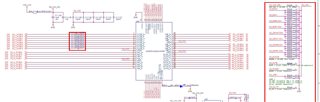
Loopback tested under the below conditions. 

FPGA High Speed IO Receiver IP : D0_I_PCIEp/N*

FPGA High Speed IO Driver IP : D0_O_PCIEp/N*

VDD_SEL : 1K-GND (3.3V mode)

ENSMB : 1K-GND(Pin-mode)

RATE : Float(Default)

SD_TH : Float(default)

LPBK : 1-GND(INA to OUTB)

EQA1,EQA0 : 20K-GND, 1K-GND

DEMB1,DEMB0 : Float, 20K-GND

But Test Result is PRBS7 Level 0.01~0.02.

We changed the EQA and DEMB, but the test results did not change. 

Please Check the loopback test.

Best regards

  • Hi Louis,

    Can you please confirm with LPBK float - normal operation - you are able to get a valid output signal? Can you put your 100-ohm scope probes on OUTA and send us eye diagram at OUTA.

    We should try to do check TX side (FPGA -> INA -> OUTA) first. Once we get a valid waveform then we can try external loop back first(OUTA to INB). Then finally we should enable LPBK pin.

    Also, for some reason i am not able to read your schematic. You can contact your TI sales/FAE so they can send me your schematic.

    Regards,, nasser

  • Hi nasser

    Thanks for your support.

    We will send the schematic through FAE of TI Korea. 

    Best regards