This thread has been locked.

If you have a related question, please click the "Ask a related question" button in the top right corner. The newly created question will be automatically linked to this question.

DS90LV028A: DS90LV028A

Part Number: DS90LV028A
Other Parts Discussed in Thread: SN74AXC1T45, DS90LV027A-28AEVM

Hello,

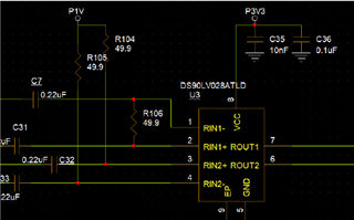
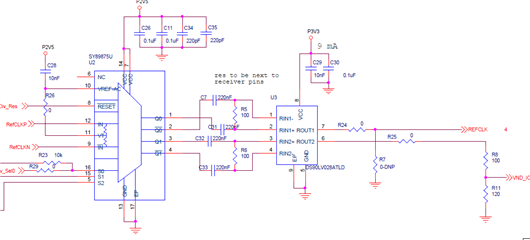
I am using the DS90LV028A to input an LVDS signal coming from a multiplexer and output a CMOS signal to other chips.

I need Rout1 as a 3V CMOS signal and Rout2 as a 1.8V CMOS signal which mandates me to add a voltage divider at the output to divide it to 1.8V on the second output.

My input voltage to the chip is 3.3V (3.21V to be accurate).

The inputs to the chip are biased to 1.25V with 50 ohm resistors.

In the picture you can find the configuration I am using . I also tried biasing with 1V instead of 1.25V.

With both inputs terminated the same (biased to 1.25V), the output never reaches 3V and sometimes, it ranges from 900mV to 2.9V and other times, it ranges 0V to 2.9V.

the AC coupled inputs are all of the same amplitude and have the same characteristics.


I would highly appreciate if you can help clarify how the circuit works and what the outputs should be when specific inputs are connected.

I am using it in many of the boards we are working on and none of them is actually providing a stable behavior.

Please correct me if you think there is anything wrong with the circuit. Also keep in mind that I am not using the configurations below together however here i am just depicting the different scenarios i tried.
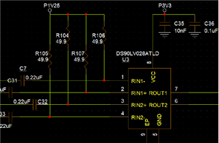
Best regards,

Christelle Saliba

  • Please find attached the picture related to the different scenarios that I mentioned above.

  • Hi Christelle,

    We have an application note detailing how to interface 3.3V LVDS receivers to lower voltage devices. Please refer to it here: https://www.ti.com/lit/an/snla307/snla307.pdf 

    Regards,

    I.K. 

  • Hello,

    Thank you for your reply.

    I checked out the application note and comparing with my circuit, the only difference is that I use a 2.5V supplied buffer that outputs the LVDS signals which I then AC couple them and bias them to 1 or 1.25V. 

    As I understand from the datasheet, the 2.5V buffer should not be any problem at all.

    After all, I measured the inputs to the driver on each pin with respect to ground and they are signals that range from 0.89V to 1.13V approximately if biased to 1V and 1.09V to 1.33V approximately if biased to 1.25V which I think is acceptable and suitable for the driver. 

    I do not understand where my problem is and why I am getting unstable behaviors at the outputs.

    Best regards,

    Christelle Saliba

  • Hi Christelle,

    What buffer are you using? Is your data DC-balanced? 50-ohm to 1V or 1.25V is not an appropriate way to terminate an LVDS signal. But regardless, AC coupling is not needed between 2.5V LVDS and 3.3V LVDS, since the common mode range of the DS90LV028A (0.2V to 3.2V) will be compatible with the output from the 2.5V LVDS. All you need is the 100-ohm differential termination on the input of the DS90LV028A, and then a level-shifter device on the output to convert the 3.3V amplitude signal to 1.8V, as detailed in the application note.

    Regards,

    I.K. 

  • Hello again,

    I am using a 1:2 LVDS output buffer, whose common mode is around 1.2V. I used an AC coupling capacitor and this is the reason why then I pulled up the bias at the input of the DS90LV028A; pulling up the bias from 0 to 1.25V.

    If you suggest that I do not use an AC coupling capacitor, I will try to remove it and test the results with a 100 ohm LVDS termination.

    Previously, before adding the pull up bias at the input of the driver, I simply had an AC coupled output with a 100 ohm resistor between the differential pairs. This was giving bad behavior at some times and this is why I proceeded with pulling up the bias. 

    The problem is that my signal is never reaching 3.3V on the output.

    As you suggested, I am already using a level shifter to convert the second output to 1.8V.

    Thank you for your support, I will get back to you should the result be better or same.

    Best regards,

    Christelle Saliba

  • Please note that the differential swing at the input of the DS90LV028A, is around 350mV. The datasheet specifies that the swing should be between 100mV and -100mV. I would highly appreciate it if you can also advise whether the swing is too big and should be reduced.

  • Hi Christelle,

    AC coupling shouldn't be used unless the data is DC-balanced. Try DC coupling and just using a 100 ohm differential termination.

    That datasheet specifies that the differential input high threshold is 100mV max , and the differential input low threshold is -100mV min. Meaning that 100mV and more is guaranteed to be high, -100mV and less is guaranteed to be low. and anything in between is indeterminate. This is how all LVDS receivers are specified according to the TIA/EIA-644A standard. 350mV swing is fine.

    Regards,

    I.K. 

  • Hello,

    I tried as you suggested and below are my results as I tested on two different circuit boards:

    1. on the first, keeping the AC coupling capacitors following the 100 ohm resistor, I received an output on the driver that ranges from 820mV to 2.84V on Rout 2 and 800mV to 2.7V on Rout 1. After removing the AC coupling caps and keeping the 100 ohm resistor, I also received a 820mV to 2.84V signal on Rout 2 and 780mV to 2.7V on Rout 1.

    2. for the second board, I did the same. With the coupling capacitor, I get a -80mV to 2.7V signal on Rout 2 and a DC offset of 2.88V on Rout 1. After removing the coupling capacitors, I also got -80mV to 2.72V on Rout 2 and also, a DC offset of 2.88V on Rout 1.

    I am not sure why in the first case i have a signal going from 800mV to 2.7V and why in the second case I am getting a somehow good signal on Rout 2 even though it doesnt reach 3.3V and just a DC offset on the Rout1.

    Best regards,

    Christelle Saliba

  • Can you share your full schematic as well as the part numbers for all the parts you're using?

    Regards,

    I.K.

  • Hello,

    kindly find the circuit below and please note that after your suggestion, I replaced C7, C31, C32, C33 by a wire.

    Best,

    Christelle Saliba

  • Hi Christelle,

    1. Please check that you're correctly configuring the mux. The datasheet says the VT should be left floating for LVDS inputs, but in your schematic it is pulled up to 2.5V 

    2. The LVDS DC electrical characteristics in the mux datasheet show a typical swing of 350 mV and and common mode voltage centered around 1.2V. This is compatible with the DS90LV028A inputs so you will not need AC coupling caps - only the differential 100-ohm resistor

    3. The resistor divider load you have on the output is demanding 15mA from the DS90LV028A outputs, which is much more than the device is able to drive (Ioh is only 0.4mA). As discussed in the application note, you should use a level translator device like the SN74AXC1T45 to level-shift the voltage

    Regards,

    I.K.

  • Hello again, 

    Regarding the VT, for sure you are correct and I will disconnect it.

    Concerning the level translator, I will try to isolate the outputs on the driver by disconnecting the transistors and checking them out for testing purposes this way I would not be forcing any current as you suggest.

    Also, I have ordered a few new driver chips which I received yesterday and that I will use to test more.

    I will get back to you as soon as I am able to perform the tests and tell you whether there is any update.

    I would like to see whether it is possible that we receive a sample evaluation board for the driver? 

    Thanks again for your resourceful support.

    Best regards,

    Christelle  

  • Hi Christelle,

    Sure, a free sample of DS90LV027A-28AEVM is available through https://tisamples.ti.com/.

    Regards,

    I.K. 

  • Hello again,

    I have received a new batch of the DS90LV028A yesterday and I used the same circuit as before (the one without the input bias and which includes R5 and R6 and the coupling capacitors). Before changing the driver chip itself I was receiving all the errors that I mentioned earlier (extremely small swing on the output, output not reaching 3 or 3.3, output with an offset of 0.88, and...), and after just replacing the chip with a new one, all the results were great, I received a range of 0 to around 3 and 3.3 V on the outputs and i was able to proceed with the circuit.

    This means that the problem was with the previously purchased drivers. Also this would make sense since other circuits were working better than those under tests now.

    Also, I would like to know what would happen if I turn off the signal coming from the U2 buffer. should I see any signal at the output of U3 like some noise or so or how should the output be when I turn off the incoming signals?

    Thanks again.

    Best regards,

    Christelle Saliba

  • Hi Christelle,

    Glad you were able to get it to function. For your other question it depends on what the output of U2 looks like when there's no input. You can reference Table 1 in the DS90LV028A datasheet for device behavior with different inputs.

    Regards,

    I.K. 

  • Hello,

    Thank you, I will check it and change accordingly. 

    Best,

    Christelle Saliba