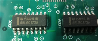
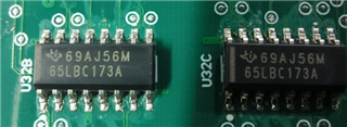
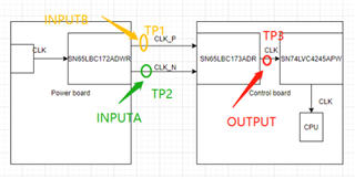
SN65LBC173ADR chip for high and low level conversion delay description
Project background
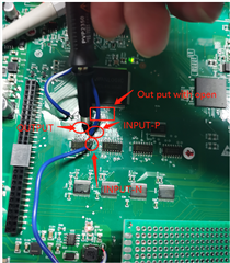
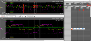
schematic diagram
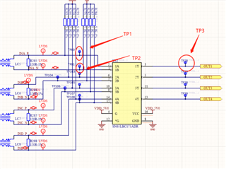
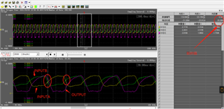
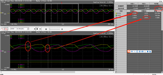
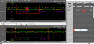
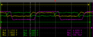
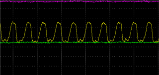
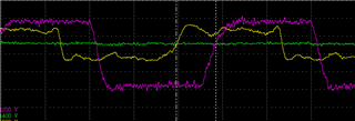
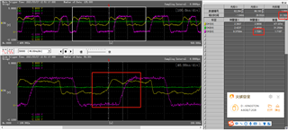
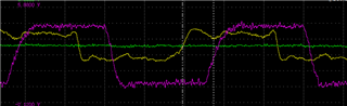
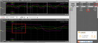
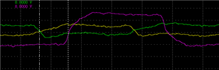
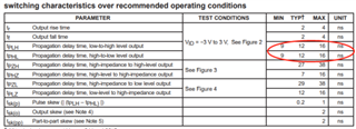
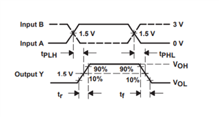
It can be seen from the chip design documents that the maximum delay of high-low level conversion is 16ns, generally 12ns, and the delay time measured by oscilloscope is 24ns. The test diagram is shown in the figure below. How to solve this problem? How to optimize the circuit is needed to reduce the delay value to the normal range.