This thread has been locked.

If you have a related question, please click the "Ask a related question" button in the top right corner. The newly created question will be automatically linked to this question.

DS90UB954-Q1: same register setting but different behavior

Part Number: DS90UB954-Q1
Other Parts Discussed in Thread: DS90UB960-Q1,

Hi TI,

we have our own designed pcb board, which has 4 pieces of 954. And we want to connect it as nvidia jetson xavier -> 954 -> 953 -> sensor.

We have a issue now, we have 2 clock src, one is 24mhz, the other one is 25mhz, and we use sync mode, 953: 0x06 -> 0x41, 0x07 -> 0x28. And when we use 24mhz, 2 cams, which connected to different 954, have different result. Cam 2 of 954(1)'s port 0 will freeze when it get 25mhz, cam 7 of 954(3)'s port 1 will not freeze. And they can both work when the clk_out of 953 is 24mhz.

And we also get the error, a FS packet was found for a virtual channel that was already in frame. An error FE packet was injected before FS was allowed through.

Two weeks ago, we tested cam 6 of 954(3)'s port 1 had issue, it will freeze when it used 24mhz, but it can work if I set clk_out of 953 as 27 mhz.

So, 25mhz INCK for sensor, cam 2 of 954(1)'s port 0 failed, cam 7 of 954(3)'s port 1 will not.

24mhz INCK for sensor, cam 2 of 954(1)'s port 0 and cam 7 of 954(3)'s port 1 -> normal, cam 6 of 954(3)'s port 0 failed.

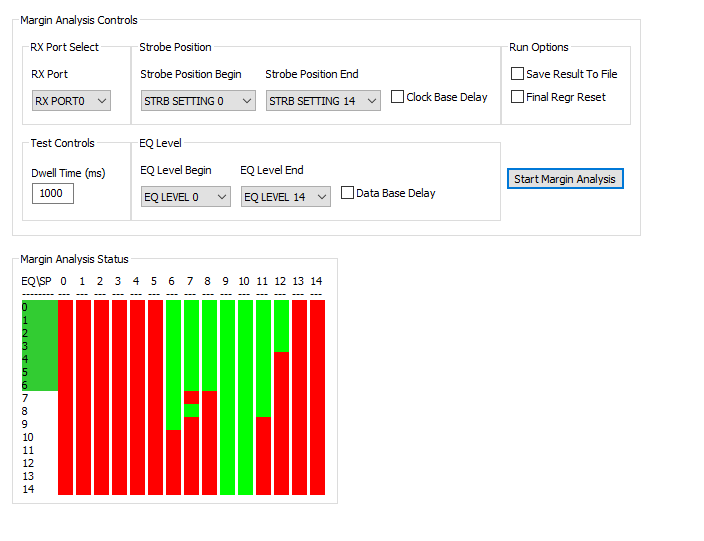
We checked lock status, 0x04 will change from 0xcf to 0xdf after starting video streaming, it should be normal. We found all of the csi error from 0x7a of 954 ( 0x7a->0x0f )

Can anyone offer some advise?

Thanks in advance

  • Hello Lihan,

    I am not sure if I understood your topology and the issue. Can you please provide a block diagram showing all SER and DES, and the REFCLK source and value of each DES. 


  • Hi Hamzeh, this is the structure of our design. We used sync mode and we have two REFCLK, one is from xavier, 24mhz, the other is an oscillator we put on the pcb board. 
    There are 3 situations, (1)refclk is 24mhz from the xavier, in 953, 0x06 is 0x41, 0x07 is 0x28. So 954/953/cam are using 24mhz. In this case, cam 2 and 7 can work, but not cam 6

    (2)refclk is 25mhz from oscillator. In 953, 0x06 is 0x41, 0x07 is 0x28. So 954/953/cam are using 25mhz. In this case, cam 7 can work, but not cam 2

    (3)refclk is 25mhz from oscillator, in 953, 0x06 is 0x6a, 0x07 is 0xb9. So 954/953 are using 25mhz, while cam is using 27mhz. In this case, cam 6 can work, but cam 2 failed 

    we used case 1 at the beginning, cam 6 will freeze when bring up. So we changed to case 2, same result on cam 6. So we changed to case 3, cam 6 can work. We thought it was the right one,so we tested other ports, it turned out case 1 is the most stable case for other port. We used same cable, serializer and sensor in these tests 

    we used same setting for sensor, only difference is the clock 

    Best regards,

    Linhan 

  • Hello linhan,

    I understood it in this way, please correct me if I am wrong:

    - All 4x DES and the Xavier are on the same board.

    - You have connected the 24 MHz coming from Xavier to all DES.

    - Also you have 1x 25MHz REFCLK connected to all DES.

    - These are all connected as in the picture, through Coax cables, to exact same serializers and exact same sensors.

    - All sensors are using the exact same configuration, resolution and data type.

    Now I have some questions:

    1) How are you switching between the 24MHz and the 25MHz to all DES at the same time?

    2) Can you measure the 24MHz and the 25MHz CLKs directly at the CLK input pins of all DES? Can you make sure that the frequency/ Amplitude/ Jitter are compliant with table 3 in the 954 d/s?

    Anothe question on your discription:

    In case (1), you said, "cam 2 and 7 can work, but not cam 6". What about other cameras?

    - Have you measured the CLKOUT from all the SER to the sensors?

    - Are the measured Clocks as expected?

    In case (2) you said, "cam 7 can work, but not cam 2". What about all other cameras?

    - Have you measured the CLKOUT from all the SER to the sensors?

    - Are the measured Clocks as expected?

    In case (3) you said, "In this case, cam 6 can work, but cam 2 failed". WHat about other cams?

    - Have you measured the CLKOUT from all the SER to the sensors?

    - Are the measured Clocks as expected?

  • Hi Hamzeh,

    (1) we used clk buffer with mux to switch the clock source for DES

    (2) the clock sources are compliant with 954. We will by pass the clock buffer and test it later

    And for case 1, all cam can be opened except cam 6, and we got the right clock

    For case 2, cam 0,3,7 can work, the others can not. 

    For case 3, I tested cam 0-3, they will freeze after bring up a few minutes, while cam 6 is stable

    Best regards,

    Linhan

  • Linhan,

    are you using synch Forwarding mode for CSI data on the 954?

  • Yes, we used synch mode for CSI data on 954

  • For using any of the synch forwarding modes, all your cameras need to be synchronized using Fsync signal. If you are not using Fsync, this will not work properly.

    Using Sync forwarding has some Requirements:
    • Video arriving at input ports should be synchronized within approximately one video line period
    • All enabled ports should have valid, synchronized video
    • Each port must have identical video parameters, including number and size of video lines, presence of synchronization packets, and so forth.

  • Hi Hamzeh. Sorry for the mistake, actually we did not set the synchronized forwarding mode. 0x21 we set as default, 0x01. What I meant should be synchronize mode, they all used same refclk

    But I'm not sure whether we did not set synchronized forwarding mode will cause this problem. We used best effort round robin

  • Okay, thanks for clarifying.

    Then I really recommend you to validate your links one after another, not all at the time.

    Your issue could be due to dividing the REFCLK or cross-talking or layout issue. By testing only one DES at once with its 2x SER, you should be able to see where is the problem coming from.

    Once you test each single DES alone, then you will start adding another DES untill you are done.

    Another idea, if possible, to test each link using our MAP Tool to see how good is your transmission link itself.

  • Hi Hamzeh. We tested current driver + serdes again, using setting like case(3) as I mentioned in previous post. And this test has been done on des 0 with 2 cameras

    There are several situation after cam0 froze. (1) 0x4d of 954(port 0) changed from 0x03 to 0x33, which indicates lock status change, but there are lock, from 0x4d[0]. (2) there will be 1 parity error first, and the streaming can still work, then multiple csi error, 0x7a from 954 will be 0x0f. Normally I can only get csi error

    And we also had the MAP test on our own design, this is the result

    Is this result acceptable?

    We are thinking that setting 0x41 => 0x6B, 0xD5=> 0x0E, 0xD4=>0X94. Is it OK for us to set 954 register like this?

    Best,

    Zheng Linhan

  • Hello Linhan,

    Yes, this result is okay.

    No, setting 0x41 = 0x6B is not a good idea. I recommend you setting it to 0xA9.

    If you want to set limits for the AEQ according to your test results, this can be done in reg 0xD5.
    you may set 0xD5 = 0x71
    But if you want to bypass the AEQ, then you can write:
    0xD4 = 0x51

  • Hi Hamzeh. Thanks for the reply.

    (1) according to the SNLA30.pdf (Margin Analysis Program (MAP) and strobe positions for DS90UB954-Q1 and DS90UB960-Q1)

    The maximum EQ should be bit [3:0] of 0xD5, and min is bit[7:4], and so is the SP min/max in 0x41. That's why we set 0x41 as 0x6B and 0xD5 as 0x0E.

    But you recommended us to set 0x41 as 0xA9 and also 0xD5 as 0x71, would you mind elaborating why setting 0x41 and 0xD5 like this?

    (2) this is the other port of our board, how should we set these register?

    (3) I just found a mistake, we set 0xD2 as 0x94 to restart AEQ, instead of setting 0xD4. But for 0xD4, if we want to bypass AEQ, only change is to set 0xD4 as 0x51? And what does EQ_STAGE_X_SELECT_VALUE means?

    Best, 

    Zheng Linhan

  • Hello Zheng,

    For the strobe position on 954 we generally recommend a range of 0xA9 for all systems as our validation testing has shown that generally regardless of the cable length and type between SER/DES, that range always falls within the allowable MAP result (assuming that the channel is meeting the FPD-Link channel requirements). For the AEQ range, generally we don't recommend limiting it unless there is a specific system level issue which we are trying to resolve by doing so. 

    In the table 3 above, there appears to be a typo for the min/max bit positions. Look at the register description and you will see it is reversed. 

    For 0xD2, setting 0x94 restarts AEQ and disables the AEQ floor setting (adaption will start from 0 instead of the programmed floor value). 0xD4 can be used to bypass AEQ and force an EQ value. Bits [7:5] control EQ stage 1 and bits [3:1] control EQ stage 2. Bit 0 enables the EQ override instead of the AEQ algorithm. 

    We do not recommend bypassing AEQ to solve a system level issue. We only recommend to use it is a debug tool during the development process. 

    It doesn't really sound like this particular issue is related to the AEQ setting based on the discussion above of failure symptoms. Have you tried enabling PATGEN from each 953 instead of the imagers as a debugging step to narrow down on where the issue is coming from?

    Best Regards,
    Casey