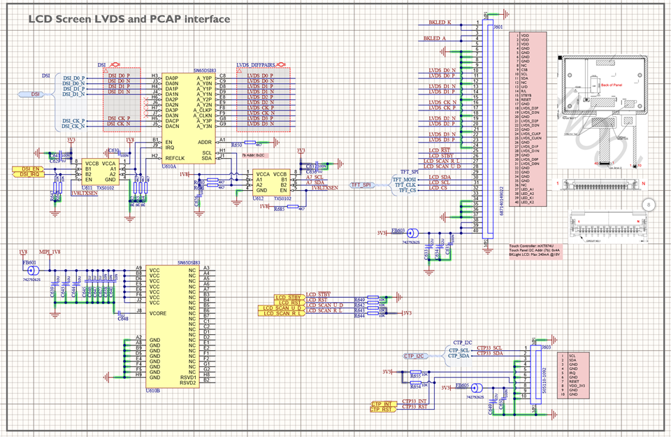
Hi
We are using SN65DSI83 to convert DSI to LVDS. Our processor only has two DSI pairs and IO voltage is 3V3.
I was wondering if you would be able to review the schematic for us? Please see attached image
Thanking you very much in advance

This thread has been locked.
If you have a related question, please click the "Ask a related question" button in the top right corner. The newly created question will be automatically linked to this question.
Hi
We are using SN65DSI83 to convert DSI to LVDS. Our processor only has two DSI pairs and IO voltage is 3V3.
I was wondering if you would be able to review the schematic for us? Please see attached image
Thanking you very much in advance

Hi Navin,
Have you checked that this device has enough throughput to support only 2 DSI data lanes? Please reference this FAQ: https://e2e.ti.com/support/interface/f/interface-forum/945185/faq-sn65dsi84-sn65dsi83-sn65dsi84-and-sn65dsi85-resolution-guide
I also recommend adding a placement for an external REFCLK for debug purposes (you can just leave it unpopulated in the BOM).
Regards,
I.K.
Hi IK
Sorry, pressed send before I finished the last post,
I was wondering if above calculations are correct? My LVDS screen max clock frequency is 50MHz and we are using 16bpp for now.
For debug external REFCLK can I use the CDCEL913PW exactly as shown in the EVK?
Otherwise, is the rest of the circuit ok?
Thanks in advance
Navin
Hi Navin,
Your calculation is correct, but the SN65DSI83 does not support 16bpp. It supports only 18bpp and 24bpp. Other than this the rest of the schematic looks okay, and yes you can use CDCEL913PW as the REFCLK.
Regards,
I.K.
Hi IK
Thank you very much for verifying schematic and confirming CDCEL913PW. I will pass on this information to my software team, regarding 16bpp not being supported by SN65DSI83.
Thanks
Navin