A related question is a question created from another question. When the related question is created, it will be automatically linked to the original question.
If you have a related question, please click the "Ask a related question" button in the top right corner. The newly created question will be automatically linked to this question.
DP83822I: 0x467 Cannot truly reflect the hardware configuration
Thank you for reaching out. You could copy the picture and insert as below.
On the hardware, can you please check if any of the other pin straps made and if those works.
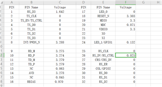
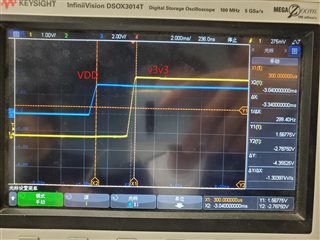
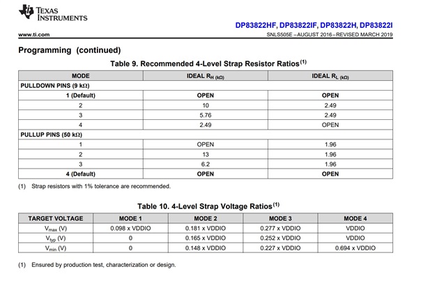
Can you please measure the voltage for the pin and the resistors values are as below.
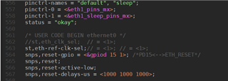
Can you please check the reset timing. If the reset is controlled by a pin, can you please do a hard reset after full boot and follow the recommended timing.
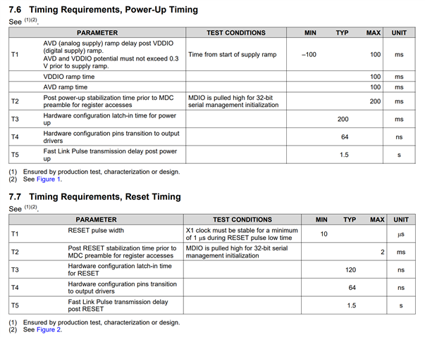
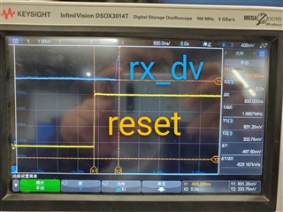
Thank for the file. The scope picture is not clear, is it indicating the pin strap level?
The 0x467 status is 2001 meaning RX_d0 and LED_0 ( reserved) pin strap is configured. Can you please check the same.
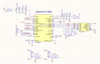
If possible, please share the schematics for review.
Also did you have a chance look into the below that i mentioned in my previous thread
On the hardware, can you please check if any of the other pin straps made and if those works.
Can you please measure the voltage for the pin and the resistors values are as below.
Can you please check the reset timing. If the reset is controlled by a pin, can you please do a hard reset after full boot and follow the recommended timing.
I looked at the schematic and measurements and have some questions
Measurements:
I assume you measured the voltage after the device came out of reset.
The Pin straps are latched during reset. Can you place the device under the reset and measure the voltage.
Schematics
I see that you connected the VDD to pin straps before the caps and connecting to vddio after the caps. I would assume the VDDIO supply ramp up would be delayed due to the caps.
The power supply needs to be table when the device comes out of reset to latch the strap configurations.
You could do this by
1. for testing, can you increase the reset to > 20ms or more and test. Based on the results you could optimize.
Alternatively
2. You can do a hard reset once the host has completed the boot assuming the power supply is stable by that time.
Thank you for the measurement, the measured voltage across RX_DV seems fine.
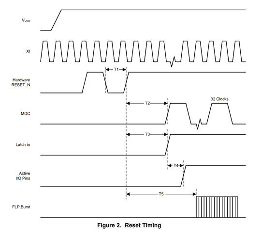
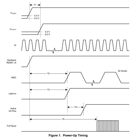
Can you please check if your are following the below timing and also toggling the reset as shown below in the reset timing after the power-up timing is complete.
Thank you. I have a questions. I measured the reset time. The MDC time(T2) is 31ms. How to measure Latch-in time(T3). Maybe T3 is just equeal to T2. That's too short a time.
The specification of 'max 2ms' seems very strange to me. it seems a strange design as puts difficult timing requirements onto a typical linux MAC. Our picture is: Ohh, the "upload" button is not found. I can't upload pictures.
Can you explain to me the time of latch-in? How to control?? Thank you.
To start with are you able to read the pin straps now? When are you trying to read the straps, during power up or later.
Regarding the timing
During power up:
Ensure the system is in reset_n till power is stabilized. Time depends on the system.
The hardware latch up time for the straps is 200ms and the MDC stabilization time is 200ms. Please provide a time of > hardware latching time before reading the register.
Reset (after power up)
After power up of the system, linux boot up, power supply stabilization, , you can toggle the reset_n for a time > 10us to do a hard reset.
The hardware latchup time for is 120ns.
The MDC stabilization time is 2ms. Please allow > 2 ms before accessing the register.
What is the initial reset time you have. If the supply ramp is slow, please increase the initial reset time. If the ethernet clock is not available, further increase the reset period.
After performing the reset of the device, are you waiting for > 200ms before reading the register?
Alternatively, After power stabilization
Can you perform a reset toggle > 10us, wait for > 10ms and read the registers. Assumption is ethernet clock is available.
Thank you Sreenivasa . I'm working fine under uboot/ Right now I'm looking for kernel-related information. I dont have EVM board, so I shouldnt be able to test loopback.


 Sreenivasa : Its too easy, "upload" is grey...RX_DV choice is Mode 3. I use this source code to read address. The result is .