This thread has been locked.

If you have a related question, please click the "Ask a related question" button in the top right corner. The newly created question will be automatically linked to this question.

DS90UB913A-Q1: Confirmation of electrical parameters when ds90ub913 gpio3 is used as clock input

Part Number: DS90UB913A-Q1

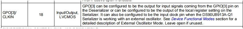
We are using ds90ub913 SerDes to use gpio3 as CLKIN function (external crystal oscillator input, frequency is 37.125mhz). At present, we encounter the following problems, in which we use VDDIO = 2.8V

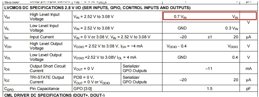
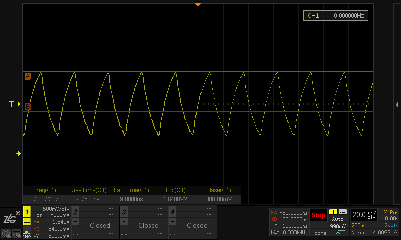
We actually measured the input signal quality of CLKIN, and found that the maximum value of CLK is only about 1.64v (the measured waveform is shown in the attachment). According to lvcmos, the following electrical properties can not reach the minimum value of VIH, but we actually tested some samples, and there is no problem

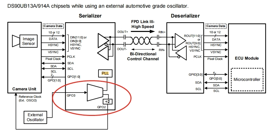
Look at the internal block diagram of the chip. When gpio3 is used as CLKIN, it is mainly used for PLL

Based on the above, I would like to ask: when gpio3 is used as clock input, what are the specific requirements of its electrical parameters? Is lvcmos level required as GPIO? Is it possible to meet the electrical property requirements of vddpll = 1.8V?


  • Hello Carl,

    This pin follows the same LVCMOS properties as the other pins so if you are using it for CLKIN, then the CLKIN signal should be adjusted to match the datasheet specs to ensure performance. I think you may be mis-interpreting the LVCMOS VIH/VIL specifications which is leading to the confusion of why it is working at all. The actual threshold voltage of the logic cell is always going to be somewhere in-between VIH min and VILmax. For example ~1V. The min/max values enable you as the system designer to ensure that across process, voltage, and temp variation of the actual VTH, your solution will work since VTH will never go outside of VIHmin and VILmax. 

    Best Regards,

    Casey