Hi Team,
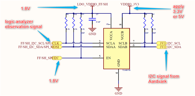
The values of pullup resistors in Figure 9 of the datasheet of TCA9617B are 240 ohms and 820 ohms. Our customer is concerned if the device would be damaged because for most I2C applications, the values of pullup resistors are in the range of kilo ohms but for this device they are less than 1k ohm.
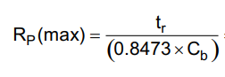
Another concern of the customer is that he connected a sensor to an Aardvark board through I2C interface. The Aardvark board is operating at 5V while the sensor is 1.8V so he used TCA9617B to interfaced the two devices. However, there are no output signal at the I2C pins on the A side (1.8V). He had confirmed that the voltage at pin 8 of TCA9617B is 5V while the pins 1 and 5 are 1.8V. He tried another 8-channel voltage level shift, LSF0108PWR, and it worked.
I understand that the TCA9617B can operate up to 5.5V but why it didn't worked in this configuration.
Regards,
Danilo