This thread has been locked.

If you have a related question, please click the "Ask a related question" button in the top right corner. The newly created question will be automatically linked to this question.

DS90UB954-Q1: Line-blanking check of CSI-2 output

Part Number: DS90UB954-Q1

Hi Team,

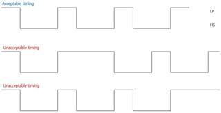
My customer is considering the design for video transmission through SerDes such as FPGA1 -> CSI-2(A) -> 953 -> 954 -> CSI-2(B) -> FPGA2. The CSI-2(A) data from FPGA1 has the fixed line-blanking like a picture below, and also CSI-2(B) data to FPGA2 has the fixed line-blanking which same as CSI-2(A). That is my customer's requirement. Is there any problem on this case? Please let me know it.

Regards,

  • Hello Jeffrey,

    The 954 CSI-2 output does not necessarily maintain specific LPS timing in the horizontal packet structure when forwarding CSI-2. The CSI-2 data is forwarded at a fixed lane rate (ex. 400, 800, 1600Mbps/lane) and then will return to LP11 while waiting for the next line to be available. So if the 953 CSI-2 input lane rate and the 954 output CSI-2 lane rate are not exactly the same (most likely case) then the LPS time between lines on the CSI-2 (A) and CSI-2 (B) would not be the same. This is a typical case for CSI-2, and it is unusual that this type of data pipieline would cause any issues within the framework of the MIPI CSI-2 protocol 

    Best Regards,

    Casey 

  • Hi Casey,

    Thanks for your kind response. I have one more question. If the 953 CSI-2 input lane rate and the 954 output CSI-2 lane rate are same, the LPS time between lines on the CSI-2 (A) and CSI-2 (B) would be same? FPGA2 can be received CSI-2 which has the constant LPS time like a picture below due to the internal line buffer of FPGA2. Please let me know it.

    Regards,

  • Hello Jeffrey,

    The LPS time may not be exactly the same between A and B, but it should be very similar if the CSI-2 lane speeds are the same. The minor difference comes from DPHY timing parameters which control the different periods of transition between lane states. However this is normal and should not cause any issue for the FPGA if it has a DPHY compliant receiver. The timing between HS/LP is at least consistent at point A or B. It will not change like the pictures that you show for unacceptable timing from line to line 

    Best Regards,

    Casey  

  • Hi Casey,

    Thanks for your kind explanation. It will help me understand this issue very well.

    Regards,