Other Parts Discussed in Thread: TDA2SX
Hi team,
1. How to apply the 0x27[3] & 0x27[5] of the register? Does the timing of PDB and GPIO2 satisfy the need to set this register?
Are there any documentation on PDB and GPIO2 issues; and precautions;
2. GPIO2 and GPIO3 of DS90DB933 are used as clock input and output pins;
What is the difference between the reference external clock and the internal PLL in the application? We now plan two options as follows:
①1920(H)*720(V)*30pfs*1.15(blanking)*2 (one pixel occupies two bytes)=95.4MHZ
②1920(H)*720(V)*28pfs*1.1(blanking)*2 (one pixel occupies two bytes)=85MHZ
When the PICLK reaches what level, TI recommends using an external crystal oscillator?
3. Can you provide us with the register configuration file of DS90DB933?
SOC: TDA2SX, video resolution: 1920*720*28pfs, format YUV422;
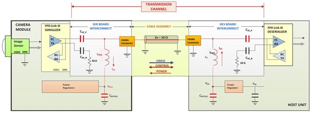
4. Is the arrangement of C(AC_N)+50ohm close to the Serdes end or does it need to be coupled to the Fakra connector end in parallel with the LVDS+ trace?
5. Are there any differences between FPD-LINKIII and FPD-LINK V for the above layout?