This thread has been locked.

If you have a related question, please click the "Ask a related question" button in the top right corner. The newly created question will be automatically linked to this question.

TPS65987D: Support request for display port feature bring up

Part Number: TPS65987D
Other Parts Discussed in Thread: TUSB1146, TUSB1064

We're facing on the problem display port feature doesn't work in our newly developed device using TPS65987D, TUSB1046 and TUSB1164.

Hardware is configured as an attached block diagram. 

PDC_USBSWITCH_ForDP_210409.pdf

As you see, we are using two PD controller (TPS65987D) and switch IC (TUSB1046 and TUSB1164) for DeMUX and MUX USB-SS signals and supporsing following sequence.

(#1) Exnternal display connect

(#2) HPD detected via CC line and PDContoller-2 set its own HPD line to high and set HPDIN of TUSB1146 to High.

(#3)MSP430 (MPU) can detect above HPD signal alternation by getting I2C-IRQ

(#4)MSP430 (MPU)  set HPD of PDController-1 to High via I2C command and set HPDIN of TUSB1064 High.

(#5)Smartphone can detect HPD via CC1 line from PDController-1 and then begin DP output.

However, we couldn't set HPD-high to PDController-1 after MPU have gotten HPD detection from PDContoller-2 when external display connected (#4 sequence doen't work).   

Culd you please check our circuit design can work for DP output and let me know the way to succesfully do #4 sequence? 

FCNT Yoshizaki

  • Yoshizaki-san,

    So looking at the diagram you have smart phone which acts as the host connected to PD1 and external monitor connected to PD2 which is a device.

    In this configuration, your DP monitor is not working or displaying - correct?

    Can you provide the project file for both PDs and its PD log taken at the host and the monitor?

    Is this always not working and does it work with other monitors?

    By the way which PD is this TPS65987DH or TPS65987DJ?

    Regards,

    Peter

  • Dear Peter-san,

    Correct PD device type we are using is TPS65987DDH.

    I'll attach PRJ file for PD1 and PD2.

    In actually, we are setting additoinal command via I2C as following after each PD contoller booting up with external SPI Flash same info written as PRJ file.

    ***I2C command setting after PD boot***

    ==================================================
    ■PD1 (UFP/Charge)
    ==================================================

    ●REG32
    0x01,0xfc,0x00,0x00,0x54,0x00,0x00,0x00,0x96,0x90,0x01,0x05,0x2c,0xd1,0x02,0x00,
    0x2c,0xb1,0x04,0x00,0x2c,0x41,0x06,0x00,0x00,0x00,0x00,0x00,0x00,0x00,0x00,0x00,
    0x00,0x00,0x00,0x00,0x00,0x90,0x01,0x00,0x00,0x00,0x00,0x00,0x00,0x00,0x00,0x00,
    0x00,0x00,0x00,0x00,0x00,0x00,0x00,0x00,0x00,0x00,0x00,0x00,0x00,0x00,0x00,0x00

    ●REG42
    0x7a,0x04,0x00,0x00

    ●REG5C
    0x07,0x00,0x0c,0x00,0x00,0x00,0x00,0x00,0x00,0x00,0x00,0x00,0x00,0x00,0x00,0x00,
    0x08,0x00,0x0c,0x00,0x00,0x00,0x00,0x00,0x00,0x00,0x00,0x00,0x00,0x00,0x00,0x00,
    0x2f,0x29,0x03,0x00,0x00,0x00,0x00,0x00,0x00,0x00,0x00,0x00,0x00,0x00,0x00,0x00,
    0x00,0x00,0x79,0x79,0x00,0x00,0x00,0x00,0x00,0x00,0x00,0x00,0x00,0x00,0x00,0x00

    ●REG77
    0x51,0x04,0x34,0x12,0x00,0x00,0x00,0x00,FW_VERSION,0x01,0x00,0x00,0x00,0x00,0x00,0x00,
    0x00,0x00,0x00,0x00,0x00,0x00,0x00,0x07

    ●REG38
    0x01,0xff,0x01,0x01,0x00,0x00,0x00,0x00,0x00,0x00,0x00,0x00,0x00,0x00,0x00,0x00

    ●REG51
    0x03,0x0F,0x08,0x08,0x00,0x02

    ●REG29
    0xc2,0x34,0x11,0x44

    ●REG27
    0x01,0x00,0x01,0x00,0x00,0x00,0x80,0x00,0x14,0x14,0x00,0x00,0x04,0x78

    ●REG28
    0xc8,0x58,0xb6,0xdf,0x01


    ==================================================
    ■PD2
    ==================================================
    ●REG32
    0x01,0xfc,0x00,0x00,0x54,0x00,0x00,0x00,0x32,0x90,0x01,0x05,0x2c,0xd1,0x02,0x00,
    0x2c,0xb1,0x04,0x00,0x2c,0x41,0x06,0x00,0x00,0x00,0x00,0x00,0x00,0x00,0x00,0x00,
    0x00,0x00,0x00,0x00,0x00,0x90,0x01,0x00,0x00,0x00,0x00,0x00,0x00,0x00,0x00,0x00,
    0x00,0x00,0x00,0x00,0x00,0x00,0x00,0x00,0x00,0x00,0x00,0x00,0x00,0x00,0x00,0x00

    ●REG42
    0x7a,0x04,0x00,0x00

    ●REG5C
    0x07,0x00,0x0c,0x00,0x00,0x00,0x00,0x00,0x00,0x00,0x00,0x00,0x00,0x00,0x00,0x00,
    0x08,0x00,0x0c,0x00,0x00,0x00,0x00,0x00,0x00,0x00,0x00,0x00,0x00,0x00,0x00,0x00,
    0x2f,0x29,0x03,0x00,0x00,0x00,0x00,0x00,0x00,0x00,0x00,0x00,0x00,0x00,0x00,0x00,
    0x00,0x00,0x79,0x79,0x00,0x00,0x00,0x00,0x00,0x00,0x00,0x00,0x00,0x00,0x00,0x00

    ●REG77
    0x51,0x04,0x34,0x12,0x00,0x00,0x00,0x00,FW_VERSION,0x01,0x00,0x00,0x00,0x00,0x00,0x00,
    0x00,0x00,0x00,0x00,0x00,0x00,0x00,0x02

    ●REG38
    0x01,0xff,0x01,0x01,0x00,0x00,0x00,0x00,0x00,0x00,0x00,0x00,0x00,0x00,0x00,0x00

    ●REG51
    0x03,0x00,0x08,0x08,0x00,0x00

    ●REG27
    0x01,0x00,0x01,0x00,0x00,0x00,0x80,0x00,0x14,0x14,0x00,0x00,0x04,0x78

    ●REG28
    0xc9,0x58,0xb6,0xdf,0x01

    ●REG29
    0x02,0x04,0x11,0x40
    ==================================================

  • Dear Peter-san,

    Correct part type is TPS65987DDH as PDContoller.

    I'll attach PRJ file for PD1 and PD2.

    In acutually we are setting additionaly via I2C command for as follows after each PD Contoller boot up frmo SPI Flash in which same config is written as attached PRJ file.

    ==================================================
    ■PD1 (UFP/Charge)
    ==================================================

    ●REG32
    0x01,0xfc,0x00,0x00,0x54,0x00,0x00,0x00,0x96,0x90,0x01,0x05,0x2c,0xd1,0x02,0x00,
    0x2c,0xb1,0x04,0x00,0x2c,0x41,0x06,0x00,0x00,0x00,0x00,0x00,0x00,0x00,0x00,0x00,
    0x00,0x00,0x00,0x00,0x00,0x90,0x01,0x00,0x00,0x00,0x00,0x00,0x00,0x00,0x00,0x00,
    0x00,0x00,0x00,0x00,0x00,0x00,0x00,0x00,0x00,0x00,0x00,0x00,0x00,0x00,0x00,0x00

    ●REG42
    0x7a,0x04,0x00,0x00

    ●REG5C
    0x07,0x00,0x0c,0x00,0x00,0x00,0x00,0x00,0x00,0x00,0x00,0x00,0x00,0x00,0x00,0x00,
    0x08,0x00,0x0c,0x00,0x00,0x00,0x00,0x00,0x00,0x00,0x00,0x00,0x00,0x00,0x00,0x00,
    0x2f,0x29,0x03,0x00,0x00,0x00,0x00,0x00,0x00,0x00,0x00,0x00,0x00,0x00,0x00,0x00,
    0x00,0x00,0x79,0x79,0x00,0x00,0x00,0x00,0x00,0x00,0x00,0x00,0x00,0x00,0x00,0x00

    ●REG77
    0x51,0x04,0x34,0x12,0x00,0x00,0x00,0x00,FW_VERSION,0x01,0x00,0x00,0x00,0x00,0x00,0x00,
    0x00,0x00,0x00,0x00,0x00,0x00,0x00,0x07

    ●REG38
    0x01,0xff,0x01,0x01,0x00,0x00,0x00,0x00,0x00,0x00,0x00,0x00,0x00,0x00,0x00,0x00

    ●REG51
    0x03,0x0F,0x08,0x08,0x00,0x02

    ●REG29
    0xc2,0x34,0x11,0x44

    ●REG27
    0x01,0x00,0x01,0x00,0x00,0x00,0x80,0x00,0x14,0x14,0x00,0x00,0x04,0x78

    ●REG28
    0xc8,0x58,0xb6,0xdf,0x01


    ==================================================
    ■PD2
    ==================================================
    ●REG32
    0x01,0xfc,0x00,0x00,0x54,0x00,0x00,0x00,0x32,0x90,0x01,0x05,0x2c,0xd1,0x02,0x00,
    0x2c,0xb1,0x04,0x00,0x2c,0x41,0x06,0x00,0x00,0x00,0x00,0x00,0x00,0x00,0x00,0x00,
    0x00,0x00,0x00,0x00,0x00,0x90,0x01,0x00,0x00,0x00,0x00,0x00,0x00,0x00,0x00,0x00,
    0x00,0x00,0x00,0x00,0x00,0x00,0x00,0x00,0x00,0x00,0x00,0x00,0x00,0x00,0x00,0x00

    ●REG42
    0x7a,0x04,0x00,0x00

    ●REG5C
    0x07,0x00,0x0c,0x00,0x00,0x00,0x00,0x00,0x00,0x00,0x00,0x00,0x00,0x00,0x00,0x00,
    0x08,0x00,0x0c,0x00,0x00,0x00,0x00,0x00,0x00,0x00,0x00,0x00,0x00,0x00,0x00,0x00,
    0x2f,0x29,0x03,0x00,0x00,0x00,0x00,0x00,0x00,0x00,0x00,0x00,0x00,0x00,0x00,0x00,
    0x00,0x00,0x79,0x79,0x00,0x00,0x00,0x00,0x00,0x00,0x00,0x00,0x00,0x00,0x00,0x00

    ●REG77
    0x51,0x04,0x34,0x12,0x00,0x00,0x00,0x00,FW_VERSION,0x01,0x00,0x00,0x00,0x00,0x00,0x00,
    0x00,0x00,0x00,0x00,0x00,0x00,0x00,0x02

    ●REG38
    0x01,0xff,0x01,0x01,0x00,0x00,0x00,0x00,0x00,0x00,0x00,0x00,0x00,0x00,0x00,0x00

    ●REG51
    0x03,0x00,0x08,0x08,0x00,0x00

    ●REG27
    0x01,0x00,0x01,0x00,0x00,0x00,0x80,0x00,0x14,0x14,0x00,0x00,0x04,0x78

    ●REG28
    0xc9,0x58,0xb6,0xdf,0x01

    ●REG29
    0x02,0x04,0x11,0x40


    ==================================================

  • Dear Peter-san,

    Correct part type is TPS65987DDH as PDContoller.

    I'll attach PRJ file for PD1 and PD2. 

    In acutually we are setting additionaly via I2C command for as follows after each PD Contoller boot up frmo SPI Flash in which same config is written as attached PRJ file.

    ==================================================
    ■PD1 (UFP/Charge)
    ==================================================

    ●REG32
    0x01,0xfc,0x00,0x00,0x54,0x00,0x00,0x00,0x96,0x90,0x01,0x05,0x2c,0xd1,0x02,0x00,
    0x2c,0xb1,0x04,0x00,0x2c,0x41,0x06,0x00,0x00,0x00,0x00,0x00,0x00,0x00,0x00,0x00,
    0x00,0x00,0x00,0x00,0x00,0x90,0x01,0x00,0x00,0x00,0x00,0x00,0x00,0x00,0x00,0x00,
    0x00,0x00,0x00,0x00,0x00,0x00,0x00,0x00,0x00,0x00,0x00,0x00,0x00,0x00,0x00,0x00

    ●REG42
    0x7a,0x04,0x00,0x00

    ●REG5C
    0x07,0x00,0x0c,0x00,0x00,0x00,0x00,0x00,0x00,0x00,0x00,0x00,0x00,0x00,0x00,0x00,
    0x08,0x00,0x0c,0x00,0x00,0x00,0x00,0x00,0x00,0x00,0x00,0x00,0x00,0x00,0x00,0x00,
    0x2f,0x29,0x03,0x00,0x00,0x00,0x00,0x00,0x00,0x00,0x00,0x00,0x00,0x00,0x00,0x00,
    0x00,0x00,0x79,0x79,0x00,0x00,0x00,0x00,0x00,0x00,0x00,0x00,0x00,0x00,0x00,0x00

    ●REG77
    0x51,0x04,0x34,0x12,0x00,0x00,0x00,0x00,FW_VERSION,0x01,0x00,0x00,0x00,0x00,0x00,0x00,
    0x00,0x00,0x00,0x00,0x00,0x00,0x00,0x07

    ●REG38
    0x01,0xff,0x01,0x01,0x00,0x00,0x00,0x00,0x00,0x00,0x00,0x00,0x00,0x00,0x00,0x00

    ●REG51
    0x03,0x0F,0x08,0x08,0x00,0x02

    ●REG29
    0xc2,0x34,0x11,0x44

    ●REG27
    0x01,0x00,0x01,0x00,0x00,0x00,0x80,0x00,0x14,0x14,0x00,0x00,0x04,0x78

    ●REG28
    0xc8,0x58,0xb6,0xdf,0x01


    ==================================================
    ■PD2
    ==================================================
    ●REG32
    0x01,0xfc,0x00,0x00,0x54,0x00,0x00,0x00,0x32,0x90,0x01,0x05,0x2c,0xd1,0x02,0x00,
    0x2c,0xb1,0x04,0x00,0x2c,0x41,0x06,0x00,0x00,0x00,0x00,0x00,0x00,0x00,0x00,0x00,
    0x00,0x00,0x00,0x00,0x00,0x90,0x01,0x00,0x00,0x00,0x00,0x00,0x00,0x00,0x00,0x00,
    0x00,0x00,0x00,0x00,0x00,0x00,0x00,0x00,0x00,0x00,0x00,0x00,0x00,0x00,0x00,0x00

    ●REG42
    0x7a,0x04,0x00,0x00

    ●REG5C
    0x07,0x00,0x0c,0x00,0x00,0x00,0x00,0x00,0x00,0x00,0x00,0x00,0x00,0x00,0x00,0x00,
    0x08,0x00,0x0c,0x00,0x00,0x00,0x00,0x00,0x00,0x00,0x00,0x00,0x00,0x00,0x00,0x00,
    0x2f,0x29,0x03,0x00,0x00,0x00,0x00,0x00,0x00,0x00,0x00,0x00,0x00,0x00,0x00,0x00,
    0x00,0x00,0x79,0x79,0x00,0x00,0x00,0x00,0x00,0x00,0x00,0x00,0x00,0x00,0x00,0x00

    ●REG77
    0x51,0x04,0x34,0x12,0x00,0x00,0x00,0x00,FW_VERSION,0x01,0x00,0x00,0x00,0x00,0x00,0x00,
    0x00,0x00,0x00,0x00,0x00,0x00,0x00,0x02

    ●REG38
    0x01,0xff,0x01,0x01,0x00,0x00,0x00,0x00,0x00,0x00,0x00,0x00,0x00,0x00,0x00,0x00

    ●REG51
    0x03,0x00,0x08,0x08,0x00,0x00

    ●REG27
    0x01,0x00,0x01,0x00,0x00,0x00,0x80,0x00,0x14,0x14,0x00,0x00,0x04,0x78

    ●REG28
    0xc9,0x58,0xb6,0xdf,0x01

    ●REG29
    0x02,0x04,0x11,0x40


    ==================================================

  • Dear Peter-san,

    Correct part type is TPS65987DDH as PDContoller.

    I'll attach PRJ file for PD1 and PD2.

    In acutually we are setting additionaly via I2C command for as follows after each PD Contoller boot up frmo SPI Flash in which same config is written as attached PRJ file.

  • Sorry I'll attach PRJ file.

  • Yoshizaki-san,

    Can you provide the project file using the Application GUI so there's no mistake in reviewing your settings? You should already have the GUI, but if not you can download it from https://www.ti.com/product/TPS65987D#design-development

    Also please provide the PD logs either using Total Phase PD analyzer or its equivalent.

    Is this not working with a specific monitor or any monitors?

    Regards,

    Peter

  • Dear Peter-san,

    Thank you check our project files and give us the updated files.
    However, we can't achieve DisplayPort output by our system yet.


    I will explain our current status.
    We use two TPS65897D in our system.
    The PD controller "1" is set Smartphone side.
    The PD controller "2" is set Display side.

    According to your project files, the PD controller 1 and 2 become following statement.

    When DisplayPort connected,
    1) Both the PD controller 1 and 2,
        CTL1 = "High" : Port0 DP Mode Selection Event is active.
        CTL0 = "High" : Port0 USB3 Event is active.
    2) the PD controller 2,
        HPD/GPIO[3] : DP HPD Port0 is active.
    3) the PD controller 1,
        HPD/GPIO[3] : DP HPD Port0 is non-active.


    We think if HPD/GPIO[3] at the PD controller 1 is "High", Displayport output will be correct state.
    To achieve it, how do we set the PD controller 1 register ?
    We also try to directly set "High" by the external MCU, but we don't know hot to set it.

    Best Regards,

    Hiroyuki Abe (FCNT)

  • Hi Abe-san,

    Can you try physically connect GPIO3 from PD1 to PD2? This HPD signal needs to propagate to PD1.

    Regards,

    Peter

  • Dear Peter-san,

    Thanks for your comments.

    I connected physically a GPIO3 port between PD1 and PD2. However, there is no status changing.

    So that, we maybe need to change the TPS65897D project file like a GPIO[3] I/O setting.

    Or, it maybe need to order that "Source: Smartphone" or "PD1" outputs protocol/command for DisplayPort via CC lines. 

    Could you give us any suggestion if you have comment?

    Best Regards,

    Hiroyuki Abe (FCNT)

  • Dear Peter-san,

    DisplayPort output succeed by the follow condition about PD controller 1.

    (1) 0x51 Register (DP SID Configuration) by the GUI tool

      1.  Enable Display Port SVID      “Checked”

      2.  Enable Display Port Mode 1   “Checked”

      3.  DP Port Capability                “DP UFP_D only”

      4.  Supports DP v1.3 signaling   “Checked”

      5.  Supports USB Gen 2 signaling  “Checked”

      6.  DP Receptacle Indication         “Plug”

      7.  USB2.0 Signaling Not Used      “Checked”

      8.  DFPD Receptacle or UFPD Plug Pin Assignment   “C”, “D”

      9.  UFPD Receptacle or DFPD Plug Pin Assignment   “C”, “D”

     10.  Multifunction Preferred            “Checked”

     11.  Preferred DP Role                   “Prefers UFP_D”

     12.  Force USB Configuration          “Checked”

     13.  DFP_D / UFP_D Connected      “UFP_D and DFP_D Connected”

     14.  DisplayPort Mode Auto Entry Allowed   “Checked”

    (2) HPDIN/GPIO[3] connects between PD1 and PD2.

    (3) HPDIN/GPIO[3] doesn't connect between PD1 and PD2

     Case (1) + (2) :

      DisplayPort automatically outputs successfully to the Display when Type-C/HDMI cable connected.

    Case (1) + (3) :

      DisplayPort outputs successfully to the Display when Type-C/HDMI cable connected and PD1 is reset.

      This "reset" is equal to VBUS cable insertion and removal.

    -----

    We try to check properly 0x51 setting because it is only trial setting.

    (I think 0x51 register maybe has extra setting.)

    Best Regards,

    Hiroyuki Abe (FCNT)

  • Hi Abe-san,

    Good to hear it's working.

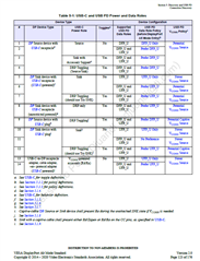
    From the above settings for DP sink (PD1), plug or receptacle should not affect. I have attached VESA spec table 5.1 here for reference.

    Setting 6 and 8 above go together, setting 13 is likely in this case.

    Connecting GPIO3 and use setting 13 should work.

    Regards,

    Peter