This thread has been locked.

If you have a related question, please click the "Ask a related question" button in the top right corner. The newly created question will be automatically linked to this question.

DS90UB941AS-Q1: Independent mode bring up

Part Number: DS90UB941AS-Q1

Dear team,

 Currently my customer uses 941's independent mode to drive two displays, display 1 is 1920*720(port 0,948) which can display normally. And the display 2 is 800*480(port 1,928) which isn't brought up yet.

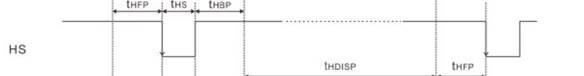
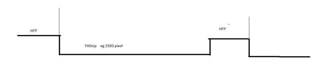
 1. We run the pattern(internal timing) on port 1 from 941 side, but display 2 still failed to display. When we connect display 1 to port 1 and run pattern(internal timing) from 941 side, and display 1 works normally. Display 2 is HV mode screen but display 1 is DE mode screen. For these two different modes, is there any different for the pattern code?

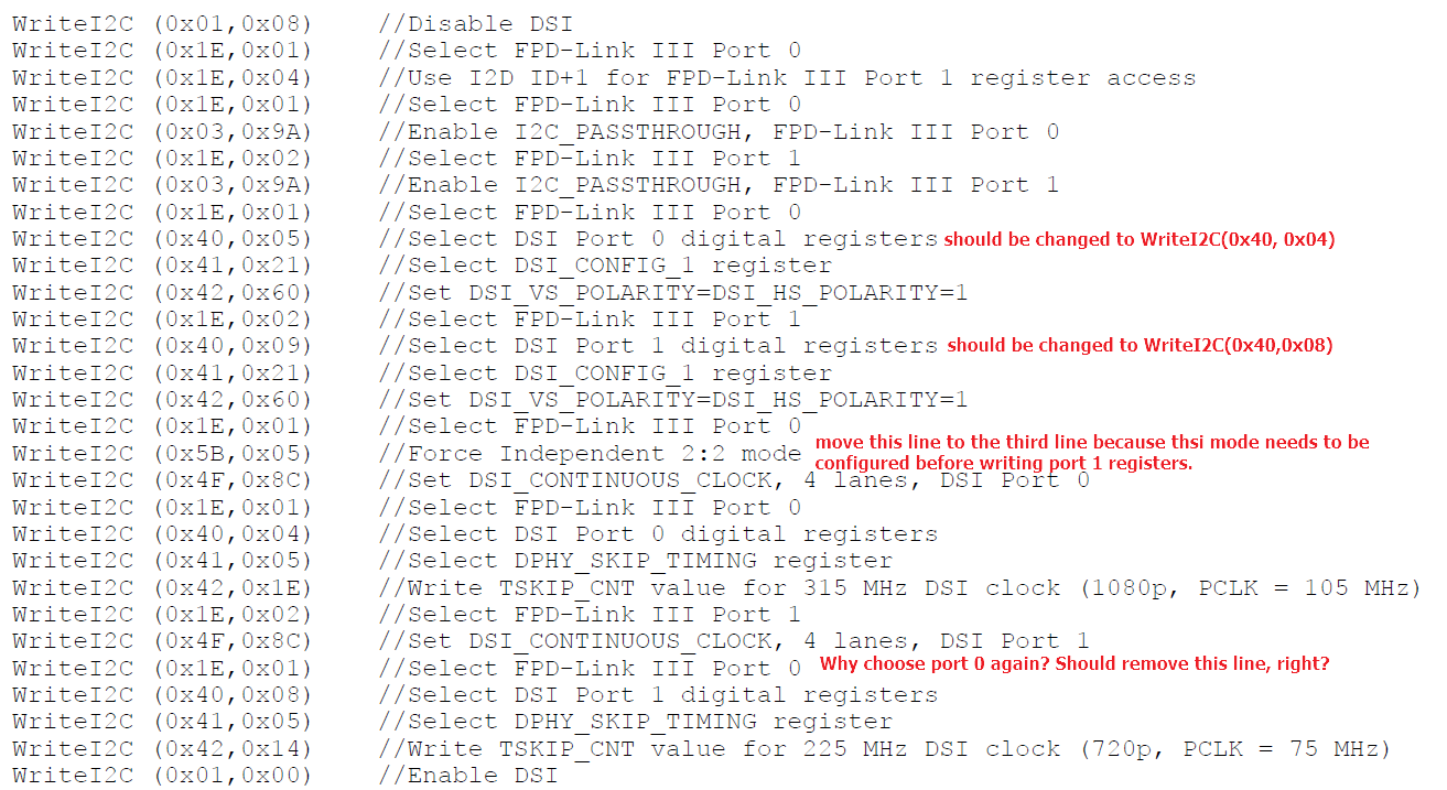
2. There is a example code for independent mode. I see some configuration is strange, could you please help check?

Thanks & Best Regards,

Sherry

  • Hi Sherry,

    As far as I know, the patgen from 941AS can be only outputted the image at a time. Basically, you can only verify the output for PORT0 then switch to PORT1, but you can't have both of them up at the same time. I am not sure if you are trying to use the SuperFrame. If it is, the smaller display will get all the vertical blanking. Please see the apps note below.

    https://www.ti.com/lit/an/snla308a/snla308a.pdf

    Aaron

  • Hi Aaron,

    According to below two description, I think the example code of independent mode should be revised. Could you please give your comments?

    Thanks & Best Regards,

    Sherry

  • Hi Sherry,

    I am not sure what you meant here to revise the description of the independent 2:2. If you have the 941AS set to independent 2:2, then the assignment is DSI0 will go to PORT0 and DSI1 go to PORT1. However, you can't have both patgen come up at the same time due to processor.

    Aaron

  • Hi Aaron,

    Sorry for the confusion. 

    My question posted yesterday is not about the pattern, and it is about our initial code. I think our initial code in the datasheet have something wrong, so I want to confirm with you.

    Please refer to the screenshot of my last post, there are four doubts,

    1. On the ninth line, WriteI2C(0x40,0x05) is a read operation instead of a write operation, but here we need a write operation, so we should change to WriteI2C(0x40,0x04);

    2. On the thirteenth line, WriteI2C(0x40,0x09) is a read operation instead of a write operation, but here we need a write operation, so we should change to WriteI2C(0x40,0x08);

    3. On the seventeenth line, WriteI2C(0x5B,0x05) should be move to third line because in our datasheet, it said 'The device will not allow writing to Port1 registers unless the device is configured for Independent 2:2 mode. Thus, Independent 2:2 mode should be enabled prior to configuring port 1 registers'. Please refer to the first screenshot.

    4. On the Fifth-to-last line, we select port 0 again, which is wrong. We should select port 1 here because port 0 has been configured on the nineteenth line.

    Thanks & Best Regards,

    Sherry

  • Hello Sherry,

    For #1 and #2 the code is correct. Bit 0 enables reads but does not disable writes. So with 0x05 you can either read or write the register. 

    For #3 the example code is also ok because the write restrictions to port 1 that you are mentioning are related to the FPD port 1, not the DSI port 1. DSI port 1 registers can be written before the part is placed into independent 2:2 mode. 

    For #4 it is also ok since this is just selecting the FPD port 0 again but it is actually not configuring anything there. It is just setting the port select pointer back to port 0 for future use. 

    By the way, 941AS actually has two pattern generator blocks to allow for independent PATGEN on port 0 and 1 in independent 2:2 mode or splitter modes. This is covered on page 124 of the datasheet. So you can select port 0 or port 1 and then configure the PATGEN parameters independently to drive two displays at once with different timing parameters. I would suggest to try this first before going to the end to end testing with the DSI source. 

    Please try this first and make sure that both displays can be brought up using PATGEN with internal timing and internal PCLK from the 941AS. If this does not work, then please post your PATGEN code as well as the panel timing for each panel so we can review and provide feedback. 

    Best Regards,

    Casey 

  • Hi Casey,

    Got it! Thanks for your detailed feedbacks!

    941 is in independent mode, and port 0 connects to 948(1920*720), and port 1 connects to 928(800*480). Currently port 0 works, and port 1 can't display, but port 1 using pattern with internal timing and internal PCLK also works. In addition, port 1 connects to the 948 display(1920*720), which can also works. Currently we are debugging the SOC's timing.

    But there is a strange thing that we can't access to the I2C of port 1 even though it works when connecting to the 948 display.

    Thanks & Best Regards,

    Sherry

  • Hello Sherry, 

    Yes, I understand. First thing I suggested to do is to generate two independent patterns from port 0 and port 1 here. For access to port 1 remote I2C, it is most likely an issue in the configuration of the I2C addresses and aliasing. Can you please provide the init code which is used? Also, what cable type is this? STP?

    Best Regards,

    Casey 

  • Hi Casey,

    Please check below initial code, thanks!

    #if 1
         write_ds90u941(ti_dev->fd, ti_dev->chip_ctrl, SER_RESET_CTL_REG, 0x08); /*disable DSI before setting */
         write_ds90u941(ti_dev->fd, ti_dev->deser_ctrl,0x1E,0x01); //Select FPD-Link III Port 0
         write_ds90u941(ti_dev->fd, ti_dev->chip_ctrl, 0x5B, 0x05); /*DUAL_CTL1 - select twisted pair cable, force independent 2:2  output mode */
         write_ds90u941(ti_dev->fd, ti_dev->deser_ctrl,0x1E,0x04); //Use I2D ID+1 for FPD-Link III Port 1 register access
         write_ds90u941(ti_dev->fd, ti_dev->deser_ctrl,0x1E,0x01) ;//Select FPD-Link III Port 0
         write_ds90u941(ti_dev->fd, ti_dev->deser_ctrl,0x03,0x9A); //Enable I2C_PASSTHROUGH, FPD-Link III Port 0
         write_ds90u941(ti_dev->fd, ti_dev->deser_ctrl,0x1E,0x02); //Select FPD-Link III Port 1
         write_ds90u941(ti_dev->fd, ti_dev->deser_ctrl,0x03,0x9A); //Enable I2C_PASSTHROUGH, FPD-Link III Port 1
         write_ds90u941(ti_dev->fd, ti_dev->deser_ctrl,0x1E,0x01); //Select FPD-Link III Port 0
         write_ds90u941(ti_dev->fd, ti_dev->deser_ctrl,0x40,0x04); //Select DSI Port 0 digital registers//modifed
         write_ds90u941(ti_dev->fd, ti_dev->deser_ctrl,0x41,0x21); //Select DSI_CONFIG_1 register
         write_ds90u941(ti_dev->fd, ti_dev->deser_ctrl,0x42,0x60); //Set DSI_VS_POLARITY=DSI_HS_POLARITY=1 //ok
         write_ds90u941(ti_dev->fd, ti_dev->deser_ctrl,0x1E,0x02); //Select FPD-Link III Port 1
         write_ds90u941(ti_dev->fd, ti_dev->deser_ctrl,0x40,0x08); //Select DSI Port 1 digital registers
         write_ds90u941(ti_dev->fd, ti_dev->deser_ctrl,0x41,0x21) ;//Select DSI_CONFIG_1 register
         write_ds90u941(ti_dev->fd, ti_dev->deser_ctrl,0x42,0x60) ;//Set DSI_VS_POLARITY=DSI_HS_POLARITY=1
         write_ds90u941(ti_dev->fd, ti_dev->deser_ctrl,0x1E,0x01) ;//Select FPD-Link III Port 0   //OK
         write_ds90u941(ti_dev->fd, ti_dev->deser_ctrl,0x4F,0x8C); //Set DSI_CONTINUOUS_CLOCK, 4 lanes, DSI Port 0
         write_ds90u941(ti_dev->fd, ti_dev->deser_ctrl,0x1E,0x01); //Select FPD-Link III Port 0  //ok
         write_ds90u941(ti_dev->fd, ti_dev->deser_ctrl,0x40,0x04); //Select DSI Port 0 digital registers
         write_ds90u941(ti_dev->fd, ti_dev->deser_ctrl,0x41,0x05); //Select DPHY_SKIP_TIMING register
         write_ds90u941(ti_dev->fd, ti_dev->deser_ctrl,0x42,0x1E); //Write TSKIP_CNT value for 315 MHz DSI clock frequency (1080p, PCLK = 105 MHz) //OK
         write_ds90u941(ti_dev->fd, ti_dev->deser_ctrl,0x1E,0x02); //Select FPD-Link III Port 1
         write_ds90u941(ti_dev->fd, ti_dev->deser_ctrl,0x4F,0x8C); //Set DSI_CONTINUOUS_CLOCK, 4 lanes, DSI Port 1 //OK
         write_ds90u941(ti_dev->fd, ti_dev->deser_ctrl,0x40,0x08); //Select DSI Port 1 digital registers
         write_ds90u941(ti_dev->fd, ti_dev->deser_ctrl,0x41,0x05); //Select DPHY_SKIP_TIMING register //ok
         write_ds90u941(ti_dev->fd, ti_dev->deser_ctrl,0x42,0x14); //Write TSKIP_CNT value for 225 MHz DSI clock frequency (720p, PCLK = 75 MHz)
         write_ds90u941(ti_dev->fd, ti_dev->chip_ctrl, 0x02, 0x01); /*DEVICE_CFG - reverse Lane lines only for port 0*/
        /*finally enable bridge device DSI */
        write_ds90u941(ti_dev->fd, ti_dev->chip_ctrl, SER_RESET_CTL_REG, 0x00);
    #endif
    #if 1 //1920X720
        write_ds90u941(ti_dev->fd, ti_dev->chip_ctrl, 0x66, 0x03);
        write_ds90u941(ti_dev->fd, ti_dev->chip_ctrl, 0x67, 0x03);
        write_ds90u941(ti_dev->fd, ti_dev->chip_ctrl, 0x66, 0x07);
        write_ds90u941(ti_dev->fd, ti_dev->chip_ctrl, 0x67, 0x80);
        write_ds90u941(ti_dev->fd, ti_dev->chip_ctrl, 0x66, 0x08);
        write_ds90u941(ti_dev->fd, ti_dev->chip_ctrl, 0x67, 0x07);
        write_ds90u941(ti_dev->fd, ti_dev->chip_ctrl, 0x66, 0x09);
        write_ds90u941(ti_dev->fd, ti_dev->chip_ctrl, 0x67, 0x2d);
        write_ds90u941(ti_dev->fd, ti_dev->chip_ctrl, 0x66, 0x04);
        write_ds90u941(ti_dev->fd, ti_dev->chip_ctrl, 0x67, 0xB0);
        write_ds90u941(ti_dev->fd, ti_dev->chip_ctrl, 0x66, 0x05);
        write_ds90u941(ti_dev->fd, ti_dev->chip_ctrl, 0x67, 0xF7);
        write_ds90u941(ti_dev->fd, ti_dev->chip_ctrl, 0x66, 0x06);
        write_ds90u941(ti_dev->fd, ti_dev->chip_ctrl, 0x67, 0x2d);
        write_ds90u941(ti_dev->fd, ti_dev->chip_ctrl, 0x66, 0x0c);
        write_ds90u941(ti_dev->fd, ti_dev->chip_ctrl, 0x67, 0x24);
        write_ds90u941(ti_dev->fd, ti_dev->chip_ctrl, 0x66, 0x0d);
        write_ds90u941(ti_dev->fd, ti_dev->chip_ctrl, 0x67, 0x8);
        write_ds90u941(ti_dev->fd, ti_dev->chip_ctrl, 0x66, 0x0a);
        write_ds90u941(ti_dev->fd, ti_dev->chip_ctrl, 0x67, 0x08);
        write_ds90u941(ti_dev->fd, ti_dev->chip_ctrl, 0x66, 0x0b);
        write_ds90u941(ti_dev->fd, ti_dev->chip_ctrl, 0x67, 0x04);
        write_ds90u941(ti_dev->fd, ti_dev->chip_ctrl, 0x66, 0x0e);
        write_ds90u941(ti_dev->fd, ti_dev->chip_ctrl, 0x67, 0x0);
        write_ds90u941(ti_dev->fd, ti_dev->chip_ctrl, 0x65, 0x07);
        write_ds90u941(ti_dev->fd, ti_dev->chip_ctrl, 0x39, 0x02);
        write_ds90u941(ti_dev->fd, ti_dev->chip_ctrl, 0x64, 0x11);
    #endif
    

    Thanks & Best Regards,

    Sherry

  • Sherry,

    This code looks like it is only setting up PATGEN for one of the FPD ports. My suggestion is to generate PATGEN on both independent FPD output ports with each port using a different target resolution to match the two displays you have. Can you also answer my question if this is STP or coax?

    Best Regards,

    Casey 

  • Hi Casey,

    Thanks for your feedback!

    The customer STP. My customer can bring up the port 1 with pattern.

    Thanks & Best Regards,

    Sherry

  • Hello Sherry,

    Ok thank, but please have them also try independent PATGEN to drive both displays with different resolutions before we move on with this debug. 

    Best Regards,

    Casey 

  • Hi Casey,

    Yes, the pattern works. We connect 941 port 1 to 926 EVM, and then test HS and VS signal. We found that there is no HS/VS signal output, so we think SOC's timing output should be wrong. My customer also want to confirm one thing, the display usually has two types, DE mode and HV mode. Does our 941 support HV mode? There is no register setting for HV MODE and DE mode in our 941 register which means we don't care the mode setting, right? DE mode or HV mode should be set in the SOC side, and our 941 support both of them, right?

    Thanks & Best Regards,

    Sherry

  • Hello Sherry,

    There is no such thing as DE mode from DSI. DSI always includes HS/VS signals, at least the sync start signal (HSS/VSS packet), but the sync end packet (HSE/VSE) is not strictly required if you are in event or burst mode. The 941AS can support all video modes supported by the DSI standard, and will always send HS/VS signals as well. If you connect to a DE mode display, then the HS/VS signals are simply ignored by the display so it can work. 

    What DSI mode is the source using for port 1? If it is event or burst mode, then the 941AS does need to be configured to set the desired HS/VS pulse widths in pixels/lines since the source will only send the start packet but not the end. 

    Best Regards,

    Casey 

  • Hi Casey,

    For your description, “ but the sync end packet (HSE/VSE) is not strictly required if you are in event or burst mode”

    Take the HS as an example, below is the typical HS signal,


    if the HSE is ignored, the HS sigal would be like below(or high/low inversed), rather than always HIGHT or always low.

    my understanding right?


    Thanks & Best Regards,

    Sherry

  • Hello Sherry,

    The above is close but not entirely correct. For 941AS in event mode:

    The SER only receives the sync start packet from the source which indicates the start of the horizontal or vertical sync and defines the blanking front porch.

    You need to set DSI_SYNC_PULSES to 0 within the 941AS in the DSI_CONFIG_0 register to ignore trying to look for the sync end packet which doesn't come from the source.  

    Then you need to program the desired sync widths into the SER using registers 0x30-0x33 in the DSI indirect page which sets the length of the HSYNC/VSYNC pulse like the first picture above. 

    The back porch is defined by the time between the end of the sync pulses that you have defined in the above regs, and the beginning of the first active line of video data. 

    The bottom line is that 941AS always needs to be configured to output sync signals no matter what to the remote source. If your display uses DE mode, then those signals are simply ignored even though they are always output from the FPD-Link devices 

    Best Regards,

    Casey