This thread has been locked.

If you have a related question, please click the "Ask a related question" button in the top right corner. The newly created question will be automatically linked to this question.

TPS25750: Application Customization Tool

Guru 29720 points

Part Number: TPS25750
Other Parts Discussed in Thread: BQ25731, ,

Hi Team,

My customer got TPS25750EVM that BQ25731 is mounted.
I understand TPS25750 Application Customization Tool includes battery charger configuration as the following.
If we using with BQ27531, there are only two settings as the following (battery charging voltage and current).


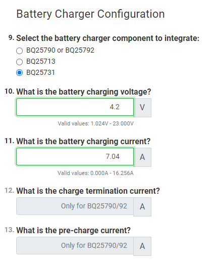
1) Do these two settings correspond to ChargeVoltage Register(05/04h) and ChargeCurrent Register(03/02h) each?
2) Does TPS25750 set only these two registers of BQ25731 when flashing the configuration to TPS25750EVM?

Best Regards,
Yaita

  • 1.  They are the ChargeVoltage Register(05/04h) and ChargeCurrent Register(03/02h) 

    2.  The TPS25750 will fully manage the BQ25731 based on the settings from the application configuration GUI.   This includes initial settings and any changes necessary because of typeC port changes.

  • Hi Chuck-san,

    Thank you for your reply.

    --------------------------------
    2.  The TPS25750 will fully manage the BQ25731 based on the settings from the application configuration GUI.   This includes initial settings and any changes necessary because of type-C port changes.
    --------------------------------
    I understand TPS25750 programs not only ChargeVoltage Register(05/04h) and ChargeCurrent Register(03/02h) with the application configuration GUI.
    Could you let me know what other registers that TPS25750 programs BQ25731 except for ChargeVoltage Register(05/04h) and ChargeCurrent Register(03/02h)?
    In addition, Is it possible to program the other BQ25731 registers with the application configuration GUI?

    Best Regards,
    Yaita

  • Yaita,

    I will need to do some research on exactly the registers that are changed.  I will get back to you early next week.

    The application configuration GUI does not allow for changing the registers programmed beyond the ones that are implemented by default.

    Regards.

    Chuck

  • Hi Chuck-san,

    Thank you for your support.
    I will wait for your feedback.

    Best Regards,
    Yaita

  • Yaita,

    A apologize that this is taking longer than expected.  I want to ensure that I have a complete list.  I am trying to separate registers that are configured once by the TPS25750 that can be overwritten from registers that are dynamically changed that should not be updated.

    I will keep you apprised of my progress.

  • Hi Chuck-san,

    I appreciate your continuous support.
    I am looking forward to your reply.

    We need to clarify the BQ25731 registers that TPS25750 accessed to.
    The following issue is one of the concerns.
    https://e2e.ti.com/support/interface/f/interface-forum/990691/tps25750evm-can-tps25750evm-sink-more-than-5a/3675237#3675237

    Best Regards,
    Yaita

  • Trigger Event Raw Data Register Update Type
    POR 0x50e00000323 0x50e00 0x00 One Time
    POR 0x1735000223 0x1735 0x35 One Time
    POR 0x64000a0006000523 0x64000a0006 0x06 One Time
    DETACH 0x1735000225 0x1735 0x35 Dynamic
    HARD RESET 0x735000224 0x735 0x35 Dynamic
    SRC_PDO1_NEG 0x11e006000327 0x11e006 0x06 Dynamic
    SRC_PDO2_NEG 0x1d7c06000328 0x1d7c06 0x06 Dynamic
    SRC_PDO3_NEG 0x273c06000329 0x273c06 0x06 Dynamic
    SRC_PDO4_NEG 0x3c0f00022d 0x3c0f 0x0f Dynamic
    POR 0x280f00022e 0x280f 0x0f One Time
    SNK_PDO1_NEG 0x3c0f00022f 0x3c0f 0x0f Dynamic
    SNK_PDO2_NEG 0x2d0f000230 0x2d0f 0x0f Dynamic
    SNK_PDO3_NEG 0x4000201032d 0x40002 0x02 Dynamic
    SNK_PDO4_NEG 0x5000201032e 0x50002 0x02 Dynamic
    DETACH 0xe000201032f 0xe0002 0x02 Dynamic
    HARD RESET 0x140002010330 0x140002 0x02 Dynamic
    PP3_SW_ON 0x640f000331 0x640f 0x0f Dynamic
    PP3_SW_OFF 0x140002000331 0x140002 0x02 Dynamic
    POR 0x3732000223 0x3732 0x32 One Time
    SNK_PDO1_NEG 0x13880400032d 0x138804 0x04 Dynamic
    SNK_PDO2_NEG 0x17700400032e 0x177004 0x04 Dynamic
    SNK_PDO3_NEG 0x1b580400032f 0x1b5804 0x04 Dynamic
    SNK_PDO4_NEG 0x1f4004000330 0x1f4004 0x04 Dynamic
    SNK_PDO5_NEG 0x232804000331 0x232804 0x04 Dynamic

    Note that the One Time registers are set once at power up and the other registers are Dynamic and can be changed with changes in the type C messages

  • Hi Chuck-san,

    Regarding the list you attached, which are BQ25731 registers that TPS25750 accessed?
    I couldn't catch it clearly.

    Best Regards,
    Yaita

  • Yaita-san,

    The Register Address is in the register section.  The number of bytes updated is in the data section.  In the excel format that I used, leading zeros are removed, so any field that only has 5 numbers should have a leading zero added  right after the 0x to byte align the data

      You can compare these two values with the 831 datasheet to extract the exact registers.

  • Chuck-san,

    I can't still understand which are BQ25731 registers that TPS25750 accessed..
    Does the list contain device address for BQ25731(6Bh)?
    Does "Register" indicate I2C address for BQ25731? For example, which is ChargeVoltage Register(05/04h) and ChargeCurrent Register(03/02h) of BQ25731?

    Best Regards,
    Yaita 

  • Yaita-san,

    To decode the table you need to break the data transactions into bytes into the TPS25731 registers.

    For example:

    The first POR event writes 05 03 00 starting at register 1.

    This will decode to 

    write 00 to register 0

    write 03 to register 1

    write 05 to register 2

    The I2C is progressive, so every additional byte is written and the register address is incremented.

  • Hi Chuck-san,

    Thank you for your continuous supports.
    It seems the first POR event writes 05 0e 00 (Data=0x50e00), so is the following correct?

    --------------------------------------------
    The first POR event writes 05 0e 00 starting at register 0.

    This will decode to 

    write 00 to register 0

    write 0e to register 1

    write 05 to register 2

    --------------------------------------------

    In addition, what does lower 3 bytes of "Raw" indicate?
    It seems "Data" is the value of "Raw" without lower 3 bytes.

    Best Regards,
    Yaita

  • Yaita,

    You are correct.  The Raw view should have been remove from the table that I provided.  It  has extra data that is not part of the data transmission.

    Regards,

    Chuck

  • Chuck-san,

    compared the first POR event (05 0e 00) with BQ25731 register.

    Regarding 01/00h register of BQ25731, the default value is "E70Eh".
    On the other hand, the first POR event program "0E00h".


    I can't understand why 01/00h register of BQ25731 should be programmed to "0E00h" and I can't believe the list you attached indicates BQ25731 register that TPS25750 accessed.
    Could you kindly check again?

    Best Regards,
    Yaita

  • Yaita,

    The engineer I work with on the BQ25731 team is out of the office until Monday.  I will verify the settings and replay back after then.  The settings that I provided are what our developers use in our firmware code.

  • Chuck-san,

    Thank you for your continuous support.
    I am looking forward to your team's feedback.

    Best Regards,
    Yaita

  • Yaita-san,

    I am still awaiting internal feedback on this issue.

    Regards,

    Chuck

  • Chuck-san,

    Thank you for following up the situation.
    I will wait for your team's feedback.

    Best Regards,
    Yaita

  • Yaita,

    I found an issue in my description of the Data.  The last byte (2 characters) is the I2C address:

    For example:

    Trigger Event Raw Data Register Update Type
    POR 0x50e00000323 0x50e00 0x00

    One Time

    The data should be interpreted as  writing 0e to register 0 and 05 to register 1.

    Regards,

    Chucj

  • Hi Chuck-san,

    Thank you for the information.

    Regarding the list you attached, could you tell me if there is meaning in the order?
    It seems TPS25750 accessed the same register (0x00/01, 0x02/03, 0x04/05, 0x06/07, 0x0f, 0x32, 0x35) and overwrited the register.

    POR 0x50e00000323 0x50e00 0x00 One Time
    POR 0x1735000223 0x1735 0x35 One Time
    POR 0x64000a0006000523 0x64000a0006 0x06 One Time
    DETACH 0x1735000225 0x1735 0x35 Dynamic
    HARD RESET 0x735000224 0x735 0x35 Dynamic
    SRC_PDO1_NEG 0x11e006000327 0x11e006 0x06 Dynamic
    SRC_PDO2_NEG 0x1d7c06000328 0x1d7c06 0x06 Dynamic
    SRC_PDO3_NEG 0x273c06000329 0x273c06 0x06 Dynamic
    SRC_PDO4_NEG 0x3c0f00022d 0x3c0f 0x0f Dynamic
    POR 0x280f00022e 0x280f 0x0f One Time
    SNK_PDO1_NEG 0x3c0f00022f 0x3c0f 0x0f Dynamic
    SNK_PDO2_NEG 0x2d0f000230 0x2d0f 0x0f Dynamic
    SNK_PDO3_NEG 0x4000201032d 0x40002 0x02 Dynamic
    SNK_PDO4_NEG 0x5000201032e 0x50002 0x02 Dynamic
    DETACH 0xe000201032f 0xe0002 0x02 Dynamic
    HARD RESET 0x140002010330 0x140002 0x02 Dynamic
    PP3_SW_ON 0x640f000331 0x640f 0x0f Dynamic
    PP3_SW_OFF 0x140002000331 0x140002 0x02 Dynamic
    POR 0x3732000223 0x3732 0x32 One Time
    SNK_PDO1_NEG 0x13880400032d 0x138804 0x04 Dynamic
    SNK_PDO2_NEG 0x17700400032e 0x177004 0x04 Dynamic
    SNK_PDO3_NEG 0x1b580400032f 0x1b5804 0x04 Dynamic
    SNK_PDO4_NEG 0x1f4004000330 0x1f4004 0x04 Dynamic
    SNK_PDO5_NEG 0x232804000331 0x232804 0x04 Dynamic


    Best Regards,
    Yaita

  • Yaita,

    That is nearly correct.  The Third POR write will access register 6,7,8, and 9.  

    POR 0x64000a0006000523 0x64000a0006
  • Chuck-san,

    Thank you for your reply.
    Regarding the list you attached, could you tell me if there is meaning in the order?
    Are they listed in the order in which TPS25750 accessed BQ25731?

    Best Regards,
    Yaita

  • Yaita,

    The order of access does not matter.  The Event utalized is the first item in the table.

  • Hi Chuck-san,

    Thank you for your answer.

    I understand the following five accesses are all sent to BQ27531 if POR is occurred.
    Is my understanding correct? 

    POR 0x50e00000323 0x50e00 0x00 One Time
    POR 0x1735000223 0x1735 0x35 One Time
    POR 0x64000a0006000523 0x64000a0006 0x06 One Time
    POR 0x280f00022e 0x280f 0x0f One Time
    POR 0x3732000223 0x3732 0x32 One Time

    Best Regards,
    Yaita