Part Number: SN65MLVD203
Other Parts Discussed in Thread: MLVD20XEVM
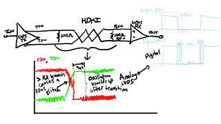
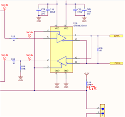
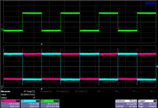
Hi, I'm seeing a small (~10-20 ns) additional output pulse when transitioning from high-to-low or low-to-high with the SN65MLVD203 transmitter and receiver used as a pair. The setup is one SN65MLVD203 configured as a transmitter over ~6 ft of HDMI cable to another SN65MLVD203 configured as a receiver. Both transmitter and receiver have 100 ohms of differential termination resistance (for a total of 50 ohms). The transmitter is provided a 0 to 3.3 V logic input from a function generator that is source terminated at 50 ohms with an SMA cable. The receiver output drives an oscilloscope with an SMA cable and is source terminated at approximately 50 ohms. Both components are powered from 3.3 V and bypassed with 0.1 uF and 10 uF of capacitance. The 0.1 uF capacitor was adjusted to 0.001 uF and 0.01 uF with no change in behavior.
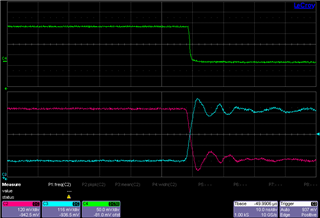
The issue is ONLY observed when transitioning below frequencies of ~25 kHz. At higher frequencies (up to 100 MHz), the extra pulse is not seen. I've identified a ~250 mV, 25 MHz common-mode oscillation on the output of the LVDS transmitter that develops across the 100 ohm resistor(s). It's like a small AC waveform riding on the digital logic voltage that the LVDS receiver will detect for transitions. This oscillation is present with or without the HDMI cable connected to the transmitter. The oscillation is not present immediately after the transmitter transitions logic states, but then builds up over a period of about 4 us . If the part is switched prior to the build-up of LVDS common-mode voltage oscillation, the glitched pulse is not detected as the transmitter oscillation has not built up and caused the receiver to detect the quick, extra transition. If the part is switched after 4 us has occurred, the oscillation rides the transitioning voltage across the receiver input and may trigger the extra 10 ns pulse at the receiver output. It is intermittent, disappears briefly after the transmitter transitions states, and is dependent on the exact phase relationship between the function generator transition and oscillating waveform phase.
I've compared the layout of my custom board to the layout of the TI reference design. Both boards have similar stack-ups and differential trace routing. One possible difference is the location of the bypass capacitor. The reference design has the bypass capacitor across the back of the chip and connected to GND and VCC with vias. My board features the capacitor off to the side of the chip.
Any help is greatly appreciated. Thank you.


