Part Number: TCA9509
Hi team
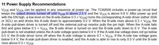
From the data sheet and other questions,
It was confirmed that it can be used with VCCA <VCCB and VCCA = VCCB.
I accidentally designed it with VCCA 3.3V and VCCB 2.5V, but I2C access is working fine.
I saw the SDA / SCL waveform of the A / B channel. The low drive is also made and the signal does not rise.
I am aware that it deviates from usage. I'm looking for a reason to support operation with VCCA> VCCB.
I want some advice.
thanks.