This thread has been locked.

If you have a related question, please click the "Ask a related question" button in the top right corner. The newly created question will be automatically linked to this question.

TUSB1064RNQEVM: how to step up the EVM

Part Number: TUSB1064RNQEVM
Other Parts Discussed in Thread: TPS65982, TUSB1064

Hi TI expert 

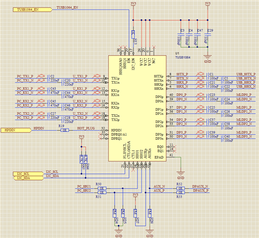
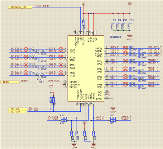
When  I use the TUSB1064RNQEVM, the USB 3.0 flash work well, but the DP interface still have some problem.

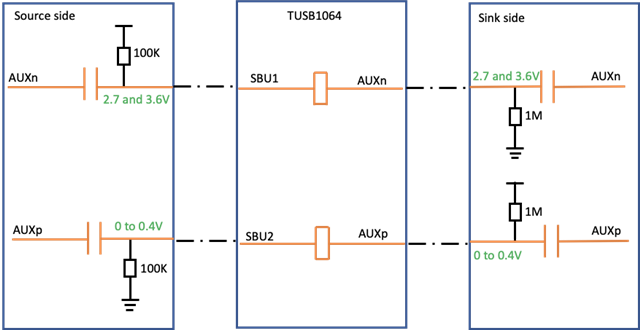
1. The  EVM default R12 and R13 resister is't soldering. and can't capture any wave form form AUXn and AUXp.

2. Then soldering the R12 and R13 with 1M resister. there are wave form from AUXp and  AUXn, but  AUXp wave form is poorly. 

3. How can I get the TUSB1064RNQEVM development step?

4. I can't search the TPS65986 data sheet, can I recommend the TPS65982 data sheet?

5. Attachment is the step record that I had do .

tusb1064EVM debug.pptx 

  • Hi,

    TPS65986 is not recommended for new designs. Instead, we suggest to use TPS65987 for the latest PD3.0 compliant device. 

    For the AUX bus, the source is AC coupled and have 100k pullup on AUXN and 100k pulldown on AUXP. The sink is also AC coupled and have 1M pulldown on AUXN and 1M pullup on AUXP. So the common mode voltage on AUXP is 0.3V and on AUXN is 3V. Since the TUSB1064EVM is between the source and the sink, there is no need to populate the pullup and pulldown on AUXP/N on the EVM. But for the TUSB1064 AUX/SBU switch, it needs to see the correct common mode voltage in order to pass AUX traffic through the switch. In this case, the common mode voltage requirement on AUXP is 0 to 0.4V and on AUXN is 2.7V to 3.6V.

    From your measurement, it looks like the pullup/pulldown is not populated correctly on the source or the sink since you are not getting the right common mode voltage. If it is possible, you can fix the pullup/pulldown on the source or the sink, or bypass the TUSB1064 and use the PD controller SBU/AUX switch and set TUSB1064 register 0x13 to 0x80 to disable AUX snooping.

    Thanks

    David

  • Hello David

    1.I found you had explain many times about the AUXn/AUXp common voltage in other thread.So I draw a  diagram according your description. Can you double check is right or not?

    2.I use TUSB1064 on myself design PCBA, and use other manufacturer PD chip the DP 2lane and USB3.0 work well so I think the EVM  DP doesn’t output signal ,it maybe consider the PD protocol whether had success build the DP alternate mode, Can you double check is right or not?


    below  table is measure on EVM board 

    Test point

    Measure valtage

    condition

    SBU1

    3.18V

    default

    SBU2

    0.04V

    default

    TUXp

    3.3V

    default

    TUXn

    3.3V

    default

    TUXp

    3.3V

    soldering  R12,R13

    TUXn

    3.3V

    soldering  R12,R13

    TUXp

    3.3V

    soldering  R4,R14

    TUXn

    3.3V

    soldering  R4,R14

    SBU1

    3.18V

    bypass 0x13=0x90

    SBU2

    1.67V

    bypass 0x13=0x90

    TUXp

    3.3V

    bypass 0x13=0x90

    TUXn

    3.3V

    bypass 0x13=0x90

  • Hi,

    I updated your block diagram to include the USB Type-C orientation switch. 

    Otherwise the pullup/pulldown resistor and calculated common mode voltage is correct.

    So the switch has to be configured correctly base on the PD communication and the common mode voltage has to be within the spec for the AUX traffic to go through correctly.

    I use TUSB1064 on myself design PCBA, and use other manufacturer PD chip the DP 2lane and USB3.0 work well so I think the EVM  DP doesn’t output signal ,it maybe consider the PD protocol whether had success build the DP alternate mode, Can you double check is right or not?

    So you are able to get DP 2 lane+USB3 work with your design, but not the DP 4 lane? Did you check to see if the TUSB1064 is being programmed correctly for DP 4 lanes?

    Thanks

    David

  • Hello David

    So you are able to get DP 2 lane+USB3 work with your design, but not the DP 4 lane? Did you check to see if the TUSB1064 is being programmed correctly for DP 4 lanes?

    >> I just try 2 lane + USB3. but not try DP 4 lane, I will try config DP 4 lane next stage.Maybe a week later.

    >> As you know, My design is follow the EVM schematic, the EVM didn't output the DP, I doubt it is the PD chip (TPS65986) didn't config the source enter alternate mode.

         My question is the TUSB1064RNQEVM's PD had config source enter  alternate mode by default factory settings? Whether should I analyze the PD protocol first ? Ensure the source enter the alternate then measure common voltage .

    Thanks

    Thomas

  • Hi, Thomas

    The TUSB1064EVM PD will negotiate for DP Alt Mode. 

    Below is the sequence I would follow.

    To check DP Alt Mode

    • Check PD protocol log file
    • Measure TUSB1064 FLIP, CTL[0:1] pin or register 0x0A, either one of them should show the TUSB1064 is being configured in USB+ 2 DP lanes or 4 DP lanes

    Check TUSB1064 HPD, is the HPD being driven high. You can force the HPD high by pulling HPD to 3.3V through a 1k resistor

    AUX common mode voltage

    • Measure common mode voltage and make sure the voltage is within spec
    • Disable AUX snoop, this will force all four DP lanes to be ON

    Check DP log file

    • Looking for possible link training failure

    Thanks

    David

  • Hello David 
    sorry to trouble you again !problem sum 20210517.pptx
    1.According your summary below link.
    https://e2e.ti.com/support/interface-group/interface/f/interface-forum/999305/faq-tusb1064-how-do-i-debug-dp-alt-mode-over-usb-type-c-interface?tisearch=e2e-sitesearch&keymatch=tusb1064#
    2.I found my AUXp line common voltage is cannot get the 0.3V, can you give some advice.
    3. Attached is the debug file that record process .
  • Hi, Thomas

    So the issue looks to be with the DP to HDMI cable you are using.

    1. Is this an active or a passive DP to HDMI cable? To support a HDMI display, you need to make sure you are using a cable that can support DP to HDMI active protocol converter.

    2. When using an active cable, R27 and R28 need to be un-populated as the 1M pullup/pulldown should be in the cable itself.

    Thanks

    David

  • Hi David

    1.According your advice I buy a Dell monitor this include the DP receptacle , and also buy the Philip DP2DP 8K cable, so the monitor can display some times.

    2.When insert the DP plug into PCBA, the Monitor model can show information at Mac os. but the monitor can’t

    show any information, still black screen. What’s the problem and how to solve?

    3.But pull out the DP plug from PCBA, the Monitor model  information still show at Mac os, so it correct or not?

    4.Some time the monitor will flash screen.

    above questions I had try to adjust the register 0x10 and 0x11 value, but the problem is still not solved, do you other

    advice?

  • Hi,

    1. For Mac still detecting the monitor after the monitor is disconnected, this looks to be a Mac issue. I would point you to this Mac link, https://discussions.apple.com/thread/251394727.

    2. Did you set bit 4 of TUSB1046 register 0x0A to a '1' and then tune the register 0x10 and 0x11? Please also disable AUX snoop by writing 0x80 to register 0x13.

    Thanks

    David

  • Hi David

    1. When I tune the register 0x10 and 0x11, I had set the bit 4 of 0x0A to a '1'.

    2. From 2. do you mean if want to tune the register 0x10 and 0x11, it should disable AUX snoop, is that right?

    3. For the device TUSB1064 AC coupling TX,RX and  SSTX, SSRX, also DP0,DP1,DP2,DP3. I used capacitors 0603 footprint ,whether the footprint will effect the signal integrity? Whether the small size like 0402 or 0201 is good for the signal integrity?

    4. Can you give some more about the DP signal chain design suggestions.

    Thanks

    Thomas 

  • Thomas

    1. Do you have a high speed scope with the DP compliance SW that you can use to verify the signal integrity? If you don't, does shorten the cable length helps? 

    2. Disabling AUX snoop is separate from the EQ tuning. By disabling the AUX snoop, I want to make sure all DP lanes are enabled.

    3. The trace width is smaller than the pad size, so there is a impedance discontinuity when going from trace to pad and pad to trace. I would recommend you go with 201 if possible to minimize the impedance discontinuity as much as possible (201 has smaller pad size comparing against the 603). What are the caps value you are currently on TX1/2, RX1/2, DP0, 1, 2, 3?

    4. Please see attached app notes on high speed layout guideline. Some info are overlapping in both guideline, but both provides good in-depth information.

    https://www.ti.com/lit/an/spraar7h/spraar7h.pdf

    https://www.intel.com/content/dam/www/programmable/us/en/pdfs/literature/ug/ug20298.pdf

    Thanks

    David

  • Hi David 

    1.I don't have a high speed scope, it's so expensive to buy it. I am try to use short cable, and still doesn't get the cable.

    2. Below is schematic and PCB layout , there are reference the TUSB1064EVM HSDC025A-002 Schematics and layout.


    3.I think the AC coupling capacitors also should consider the ESL and  ESR,  Maybe the lower ESL , ESR capacitors is best ,Do you agree with my point?

  • Thomas

    1. SSTX/SSRX is connected to the USB connector and DP is also connected to the DP connector from looking at your layout. 

    • SSTX of 100nF may be ok, but can be changed to 220nF
    • SSRX of 100nF will be an issue. With corresponding TX of 100nF, total capacitance is 50nF. This is outside of the USB spec and can cause DC wander. Please change to 330nF.
    • DP of 100nF will be an issue with the same reason as SSRX. Replace the cap with 330nF or short with 0-ohm resistor

    2. Remove 1M pullup/pulldown on AUX, the common mode voltage should be set by the source and the sink

    3. Any chance you can share the actual layout file for a detailed review?

    4. Generally speaker, lower the ESL/ESR, the better. Please refer to this link for a more detailed discussion: www.programmersought.com/.../

    Thanks
    David 

  • Hi David 

    1. According your suggestion I had update the schematic .

    • change SSTX capacitors 220nf
    • change SSRX capacitors 330nf
    • change DP AC capacitors 330nf  

    2. There is additional question How to calculate the total capacitance of USB? If SSTX is 220nf and the SSRX is 330nf, so the total capacitane is 132nf is that right?

    04Type-C to USB3.0&DP Board V0.3_58x58x1.2mm.zip

  • Thomas

    1. Correct. For two capacitors in series, the total capacitance = 1/(1/Cap1+ 1/Cap2)

    2. Looking at the layout

    • Please have ground plane filled in the circled area

    • Do you have a power plane for the 3.3V? It would good to have a plane than a trace for the 3.3V
    • The small power decoupling caps C3, C4, and C47 should be placed on the bottom of board between the 3.3V power plane and the TUSB1064 thermal pad

    I would use short DP and USB cable, change the capacitors value and size, and then see if you are able to resolve the video issue.

    Thanks
    David

  • Hello David

    Thank you very must for your great support , I will follow your suggestion to update the layout .but it will take a few days .

    1.Because of my proof knowledge and interested ,I had some questions want to ask you .

    2.How is the relationship between TUSB1064 pin AUXp , AUXn and PD protocol,I had study some documents just like https://www.ti.com/lit/an/slva844b/slva844b.pdf?ts=1622450209177 , but I still did't get the clear understand between the AUXp,AUXn and the PD protocol. can you support some documents that describe AUXp AUXn and the PD protocol ?

    Thanks 

    Thomas 

  • Hi, Thomas

    At high level, the PD will properly configure the TUSB1064 AUX/SBU switch depending on the Type-C orientation (CC1/2 normal and flip) and when enter into DP Alt Mode (PD protocol communication).

    Thanks

    David