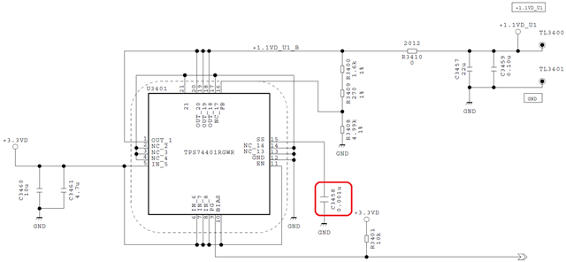
Other Parts Discussed in Thread: TPS74401, TUSB7340, TUSB1310
In rare cases, continuous noise is generated in the power supply line when the power is turned on.
(About once when the power is turned on 30 times)
When power supply noise occurs, XHCI register access (7.5.3.3.9 Port Status and Control Register) always fails.
What could be the cause of this case?
Please tell me the possible measures.
Please let me know if there is an errata regarding the power supply.
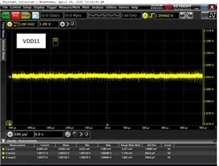
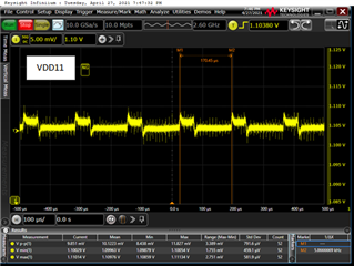
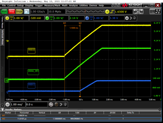
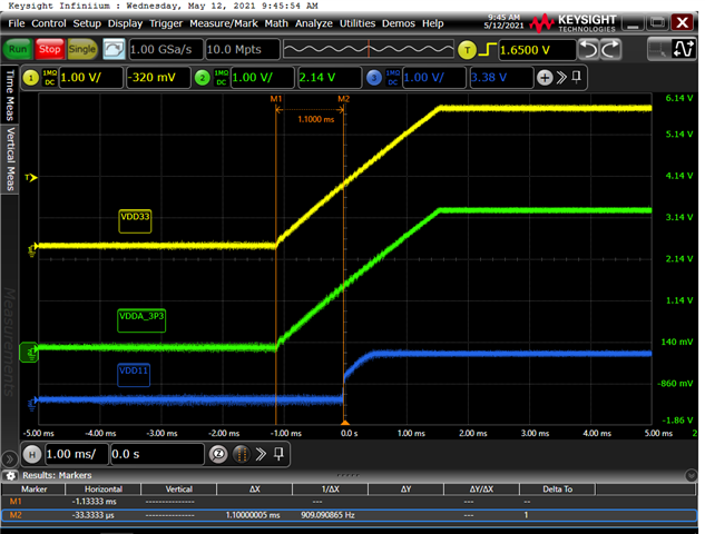
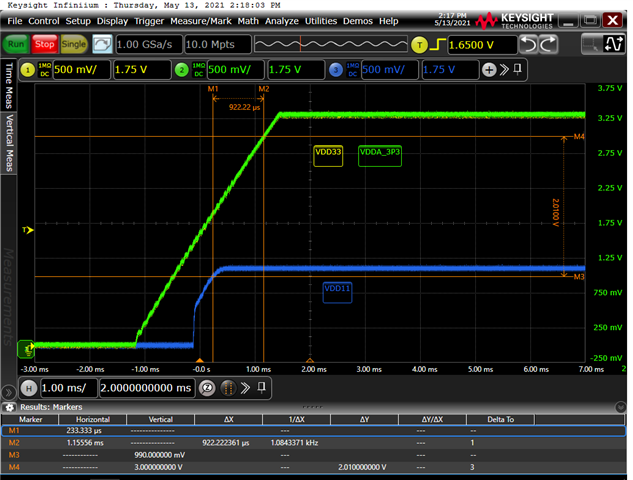
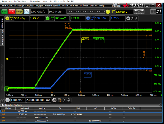
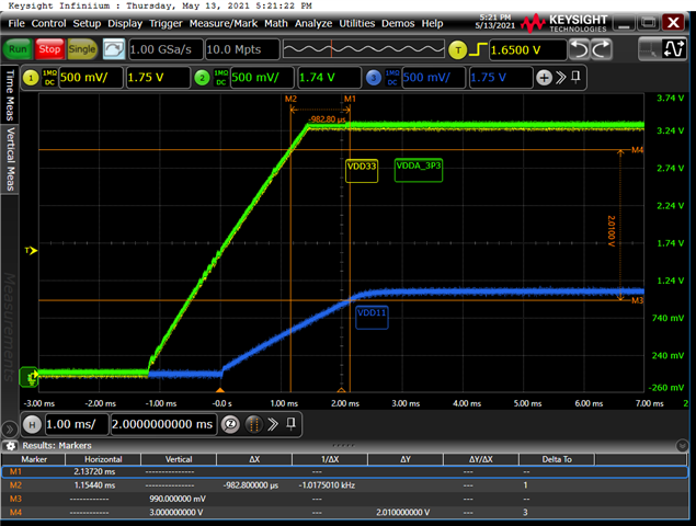
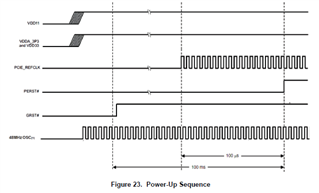
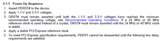
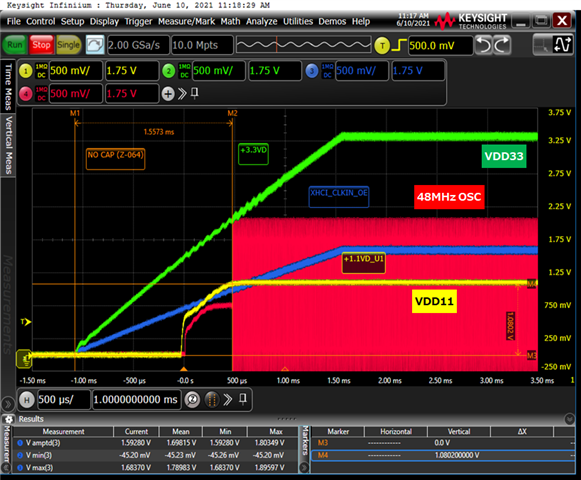
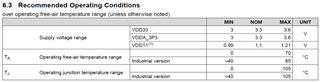
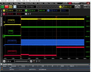
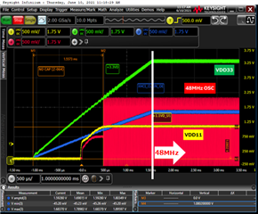
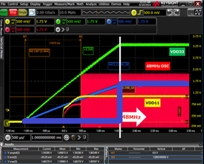
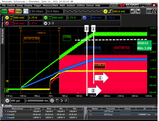
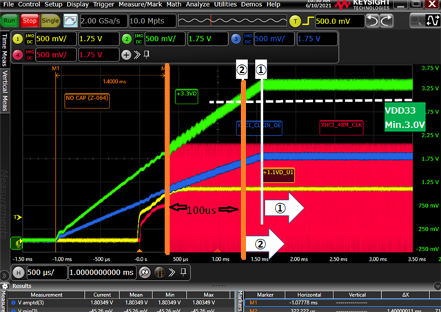
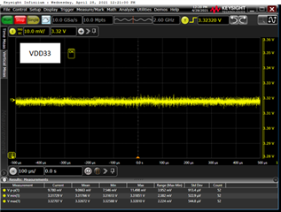
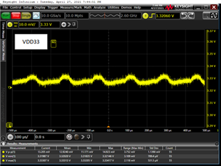
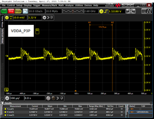
The following is the power waveform of each of the normal operation and the abnormal operation.
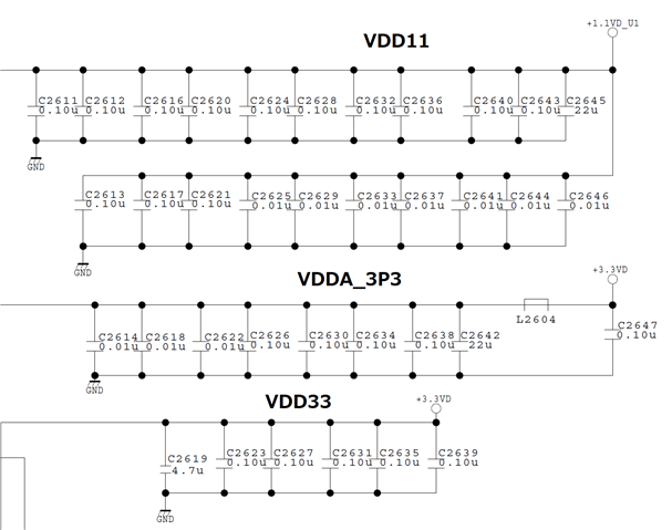
VDD33
Normal operation Abnormal operation
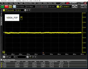
VDDA_3P3
Normal operation Abnormal operation
VDD11
Normal operation Abnormal operation