


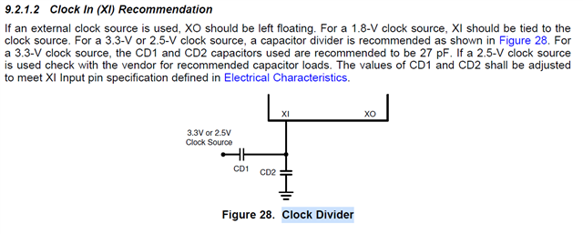
Part Number: DP83867E
Hello there,
Can I get more information on the purpose and selection of CD1 and CD2? It would be appreciated if you can share any relevant material.
Customer supplies a clock into XI pin directly from the output of SG-8101CG with 1.8V level LVCMOS while VDDIO = 1.8V. (that is, they don't implement the clock divider on XI pin) I want to check if this configuration has no issue.
