A related question is a question created from another question. When the related question is created, it will be automatically linked to the original question.
If you have a related question, please click the "Ask a related question" button in the top right corner. The newly created question will be automatically linked to this question.
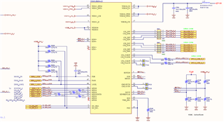
Since VDD_SEL = LOW, make sure that each VDD11 pin group has a separate set of 4.7uF/0.01uF capacitors to GND, to ensure stable power. Do not connect a 1.1V supply rail to the VDD11 pins. Just terminate to GND with capacitors. An internal voltage regulator is used. See datasheet for the Internal 1.1-V reference schematic.
For the VDDIO and VDD18 pins, see the datasheet or UB954 EVM User's Guide for the specific capacitors that should be used at each pin. Populate each set of power pins with a separate set of capacitors to ensure stable power.
At the PDB pin, TI recommends using a SW Control method (microcontroller), to have greater control over when PDB goes HIGH (see Power-Up Sequencing in the datasheet). If you want to use the HW Control option, use a 33kOhm pull-up resistor and >10uF capacitor to GND.
The PASS and LOCK pins are output pins, which indicate a LOCK/PASS status and are typically routed to a processor's input or a test point. Remove the pull-up resistors to these 2 pins.
On GPIO3/INTB, make sure to use a 4.7kOhm pull-up resistor to VDDIO if you are planning on using the INTB functionality in this shared pin.
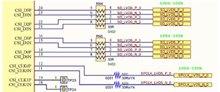
On the CSI-2 lanes, make sure to remove the CMCs. Your current configuration will not work, since CSI-2 is not always differential.
For CMLOUT P/N monitoring, terminate with a 100ohm differential load across the pins. And consider adding 33nF capacitors at each pin. Reference the "DS90UB95x-Q1EVM Deserializer User's Guide" for an example schematic.
For the XOUT and XIN/REFCLK pins, the load capacitor values will mainly depend on the vendor information of the crystal used. See Section 7.4.4 and 7.4.5 in the datasheet for TI's recommendations.
Pin 44 (RES) can be tied directly to GND, since there is no scenario where a voltage needs to be applied here, and thus no need for a pull-down resistor.