Other Parts Discussed in Thread: TSB82AA2
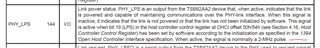
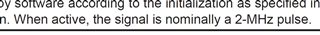
Hi, I am currently developing a board using 3 - TSB41BA3F-EP devices to receive data from a 3rd party IEEE 1394b simulator equipment. The data from the equipment is received by the PHYs TPA/TPB side (transformer coupled with PULSE TM1062TXHUA), and sent via the D0-D7 interface to an FPGA acting as a LLC device. While doing tests at higher temperature (70C ambient), we noticed that the data on the PHYs parallel bus stops and the STOI bit register on address 0101 is set as well as bus resets been generated. The PCLK signal doesn't seem to stop, only the data. We are trying to understand why this is happening since we cannot find any more information on the datasheet explaining the possible conditions that are setting this bit to stop data flow.
.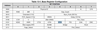
Here are the values of the registers before and after temperature rise
|
Room Temp |
|
High Temp |
||||
|
PHY1 |
PHY2 |
PHY3 |
|
PHY1 |
PHY2 |
PHY3 |
|
c10 - 00006000 |
1010 - 00006000 |
1410 - 00006000 |
|
c10 - 00006000 |
1010 - 00006000 |
1410 - 00006000 |
|
c10 - 0000613f |
1010 - 0000613f |
1410 - 0000613f |
|
c10 - 0000613f |
1010 - 0000613f |
1410 - 0000613f |
|
c10 - 000062e3 |
1010 - 000062e3 |
1410 - 000062e3 |
|
c10 - 000062e3 |
1010 - 000062e3 |
1410 - 000062e3 |
|
c10 - 000063eb |
1010 - 000063eb |
1410 - 000063eb |
|
c10 - 000063eb |
1010 - 000063eb |
1410 - 000063eb |
|
c10 - 00006480 |
1010 - 00006480 |
1410 - 00006480 |
|
c10 - 00006480 |
1010 - 00006480 |
1410 - 00006480 |
|
c10 - 00006510 |
1010 - 00006510 |
1410 - 00006510 |
|
c10 - 00006518 |
1010 - 00006518 |
1410 - 00006518 |
|
c10 - 00006610 |
1010 - 00006610 |
1410 - 00006610 |
|
c10 - 00006610 |
1010 - 00006610 |
1410 - 00006610 |
|
c10 - 00006700 |
1010 - 00006700 |
1410 - 00006700 |
|
c10 - 00006700 |
1010 - 00006700 |
1410 - 00006700 |
|
c10 - 000068f6 |
1010 - 000068f6 |
1410 - 000068f6 |
|
c10 - 000068fe |
1010 - 000068f6 |
1410 - 000068fe |
|
c10 - 00006940 |
1010 - 00006940 |
1410 - 00006940 |
|
c10 - 00006940 |
1010 - 00006940 |
1410 - 00006940 |
|
c10 - 00006a2a |
1010 - 00006a2a |
1410 - 00006a2a |
|
c10 - 00006a2a |
1010 - 00006a2a |
1410 - 00006a2a |
|
c10 - 00006b08 |
1010 - 00006b08 |
1410 - 00006b08 |
|
c10 - 00006b08 |
1010 - 00006b08 |
1410 - 00006b08 |
|
c10 - 00006c0e |
1010 - 00006c1f |
1410 - 00006c11 |
|
c10 - 00006c02 |
1010 - 00006c03 |
1410 - 00006c02 |
|
c10 - 00006d00 |
1010 - 00006d00 |
1410 - 00006d00 |
|
c10 - 00006d00 |
1010 - 00006d00 |
1410 - 00006d00 |
|
c10 - 00006e00 |
1010 - 00006e00 |
1410 - 00006e00 |
|
c10 - 00006e00 |
1010 - 00006e00 |
1410 - 00006e00 |
|
c10 - 00006f1d |
1010 - 00006f1d |
1410 - 00006f1d |
|
c10 - 00006f1d |
1010 - 00006f1d |
1410 - 00006f1d |
The current setup we are using for the Port Speed / Mode selections is MODE1 as shown on Table 5-1 on the datasheet.
I can provide a schematic if needed to check the pinout setting.
Thanks for the help with this issue.
Francisco