This thread has been locked.

If you have a related question, please click the "Ask a related question" button in the top right corner. The newly created question will be automatically linked to this question.

TIC12400-Q1: TIC12400: Wakeup configuration issues

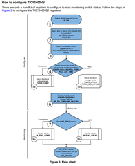
Part Number: TIC12400-Q1
Other Parts Discussed in Thread: TIC12400

Hello Team

I have configured the TC12400 and it works fine for both analog and digital inputs reading.

I have configured IN0 and IN1 to Analog inputs mode, IN2 and IN13 to Digital inputs.

I'm tried configuring them as wake sources but only IN2 works, others not working.

1. For IN13 - Configured same as IN2 but not working. Any additional settings to be done for IN13 compared to IN2.

2. For IN0 and IN1 - while debugging I found that the threshold registers not updating 0's.

Could you please provide the Analog input registers setting sequence for wakeup functionality.

Thank you

Santosh

  • Hi Santosh,

    Generally speaking you will need to have the VS and VDD supplies ON and stable at all times.  You will also need to enable the input for interrupt generation with the INT_EN_CFGx registers and set the edge type for the switch that will generate an interrupt in the INT_EN_COMPx registers.

    I can help you configure the registers, but I have a few questions about your configuration.

    1. What is your VS voltage?  Is it always ON and stable?
    2. What is your VDD voltage?  Is it always ON and stable?
    3. Are your switches connected to VS or to GND?
    4. Are your switches normally open or closed (or will the inputs be normally high or low, etc.?)
      1. Basically, are we looking for a rising edge, falling edge, or either edge type of interrupt?

    Can you either provide me with the registers values you are using in your setup or answer the following questions?

    1. Are you sourcing or sinking current on the inputs, or neither (0mA option).
    2. How much current are you sourcing or sinking on the inputs?
    3. What are the comparator threshold voltages used with the digital inputs?
    4. What are the ADC thresholds used and their settings?
    5. What is the value of your Interrupt configuration registers 0x22 - 0x28)?

    As of now, I don't know how to configure the INT_EN_CFGx and INT_EN_COMPx registers for your application.  Once I know more, I can provide some specific values.

    Regards,

    Jonathan

  • Hi Jonathan

    Thank you for the quick response. I have sent an e-mail about the configuration and other details.

  • Here is my configuration

    /* Step1: Enable channels */
    /**
    * IN_EN Register 1Bh:
    * Enable Input Channels - 00, 01, 02, 06, 08, 13, 14
    */
    data_w[0] = 0x00u;
    data_w[1] = 0x61u;
    data_w[2] = 0x47u;
    return_val |= tic12400_reg_write(
    APP_TIC12400_DEVICE0,
    TIC12400_IN_EN_R,
    data_w);

    /* Step2: Current Source Selection */
    /**
    * CS_SELECT 1Ch: Current Source/Sink
    * Configure all to source selection [0h]
    */
    data_w[0] = 0x00u;
    data_w[1] = 0x00u;
    data_w[2] = 0x00u;
    return_val |= tic12400_reg_write(
    APP_TIC12400_DEVICE0,
    TIC12400_CS_SELECT_R,
    data_w);

    /* Step3: Wetting Current Configuration */
    /**
    * WC_CFG0 Register 1Dh: Wetting current
    * Configure to 2mA [2h]
    */
    data_w[0] = 0x01u;
    data_w[1] = 0x20u;
    data_w[2] = 0x12u;
    return_val |= tic12400_reg_write(
    APP_TIC12400_DEVICE0,
    TIC12400_WC_CFG0_R,
    data_w);

    /**
    * WC_CFG1 Register 1Eh: Wetting current
    * Configure to 2mA [2h]
    */
    data_w[0] = 0x00u;
    data_w[1] = 0x00u;
    data_w[2] = 0x12u;
    return_val |= tic12400_reg_write(
    APP_TIC12400_DEVICE0,
    TIC12400_WC_CFG1_R,
    data_w);

    /* Step4: Mode Selection */
    /**
    * Mode Register 32h:
    * Pins 00, 01, 08 are configured for Analog Inputs.
    * All other pins are configured for Digital Inputs.
    */
    data_w[0] = 0x00u;
    data_w[1] = 0x01u;
    data_w[2] = 0x03u;
    return_val |= tic12400_reg_write(
    APP_TIC12400_DEVICE0,
    TIC12400_MODE_R,
    data_w);

    /* Step5: Set Device Configuration */
    /**
    * CONFIG Register 1Ah:
    * Set trigger to 0 [Stop device]
    * VS Ratio to 1 - to support voltage range from 4.5V to 30V
    * polling disabled.
    * INT_CONFIG -- Interrupt Assertion to static
    * crc disabled
    * Polling activation time 1024us [Bh]
    * Polling time 4ms [1h]
    */
    data_w[0] = 0x81u;
    data_w[1] = 0x25u;
    data_w[2] = 0x62u;
    return_val |= tic12400_reg_write(
    APP_TIC12400_DEVICE0,
    TIC12400_CONFIG_R,
    data_w);

    /* Step6: Comparator Thresholds Configuration */
    /**
    * THRES_COMP Register 21h:
    * Set to 2h - threshold voltage to 3V
    * Digital Inputs - 02, 06, 13, 14
    */
    data_w[0] = 0x00u;
    data_w[1] = 0x00u;
    data_w[2] = 0x8Au;
    return_val |= tic12400_reg_write(
    APP_TIC12400_DEVICE0,
    TIC12400_THRES_COMP_R,
    data_w);

    /* Step7: Enable global interrupt on state change */
    /**
    * INT_EN_CFG0 Register 24h: Global Interrupt
    * SSC_EN to enable interrupt assertion on Switch State Change [SSC]
    */
    data_w[0] = 0x00u;
    data_w[1] = 0x00u;
    data_w[2] = 0x04u;
    return_val |= tic12400_reg_write(
    APP_TIC12400_DEVICE0,
    TIC12400_INT_EN_CFG0_R,
    data_w);

    /* Step8: Analog Thresholds Configuration */
    /**
    * THRES_CFG0 Register 29h:
    * Configure THRES0 to ~2.6V [1B9h]
    */
    data_w[0] = 0x00u;
    data_w[1] = 0x01u;
    data_w[2] = 0xB9u;
    return_val |= tic12400_reg_write(
    APP_TIC12400_DEVICE0,
    TIC12400_THRES_CFG0_R,
    data_w);

    /**
    * THRES_CFG1 Register 2Ah:
    * Configure THRES0 to ~2.6V [1B9h]
    */
    data_w[0] = 0x00u;
    data_w[1] = 0x01u;
    data_w[2] = 0xB9u;
    return_val |= tic12400_reg_write(
    APP_TIC12400_DEVICE0,
    TIC12400_THRES_CFG1_R,
    data_w);

    /**
    * TIC12400_THRESMAP_CFG0_R Register 2Eh:
    * Configure Analog Inputs Threshold to THRES2
    */
    data_w[0] = 0x00u;
    data_w[1] = 0x00u;
    data_w[2] = 0x12u;
    return_val |= tic12400_reg_write(
    APP_TIC12400_DEVICE0,
    TIC12400_THRESMAP_CFG0_R,
    data_w);

    /**
    * TIC12400_THRESMAP_CFG1_R Register 2Fh:
    * Configure Analog Inputs Threshold to THRES2
    */
    data_w[0] = 0x00u;
    data_w[1] = 0x00u;
    data_w[2] = 0x12u;
    return_val |= tic12400_reg_write(
    APP_TIC12400_DEVICE0,
    TIC12400_THRESMAP_CFG1_R,
    data_w);

    /* Step9: Interrupts detection configuration */
    /**
    * INT_EN_COMP1 Register 22h: Enable Interrupts
    * Set interrupt generation on both rising and falling edges - 3h.
    * Digital Inputs : 02, 06
    */
    data_w[0] = 0xffu;
    data_w[1] = 0xffu;
    data_w[2] = 0xffu;
    return_val |= tic12400_reg_write(
    APP_TIC12400_DEVICE0,
    TIC12400_INT_EN_COMP1_R,
    data_w);

    /**
    * INT_EN_COMP2 Register 23h: Enable Interrupts
    * Set interrupt generation on both rising and falling edges - 3h.
    * Digital Inputs : 13, 14
    */
    data_w[0] = 0xffu;
    data_w[1] = 0xffu;
    data_w[2] = 0xffu;
    return_val |= tic12400_reg_write(
    APP_TIC12400_DEVICE0,
    TIC12400_INT_EN_COMP2_R,
    data_w);

    /**
    * INT_EN_CFG1 Register 25h: Enable Interrupts
    * Set interrupt generation on both rising and falling edges - 3h.
    * Analog Inputs : 00, 01, 08
    */
    data_w[0] = 0xffu;
    data_w[1] = 0xffu;
    data_w[2] = 0xffu;
    return_val |= tic12400_reg_write(
    APP_TIC12400_DEVICE0,
    TIC12400_INT_EN_CFG1_R,
    data_w);

    /* Step10: Enable Device to Start Operation */
    /**
    * Now all the required settings done, enable trigger
    * for normal operation.
    *
    * CONFIG Register 1Ah:
    * Set trigger to 1 for Normal operation.
    */
    data_w[0] = 0x81u;
    data_w[1] = 0x2Du;
    data_w[2] = 0x62u;
    return_val |= tic12400_reg_write(
    APP_TIC12400_DEVICE0,
    TIC12400_CONFIG_R,
    data_w);

    /* Step11: Clear Interrupts */
    /**
    * Clear all the interrupts by reading Interrupt Status Register
    * before jumping to the task.
    */
    return_val |= tic12400_reg_read(
    APP_TIC12400_DEVICE0,
    TIC12400_INT_STAT_R,
    tic12400_int_stat_r);

  • What is your VS voltage? Is it always ON and stable? ==> 12V. it's stable. VS1 and VS2 connected to Battery.
    What is your VDD voltage? Is it always ON and stable? ==> 3.3V. it's stable.
    Are your switches connected to VS or to GND? ==> Gnd
    Are your switches normally open or closed (or will the inputs be normally high or low, etc.?) ==> open
    Basically, are we looking for a rising edge, falling edge, or either edge type of interrupt? ==> both edges
    Can you either provide me with the registers values you are using in your setup or answer the following questions? ==> see attached

    Are you sourcing or sinking current on the inputs, or neither (0mA option). sourcing, 2mA
    How much current are you sourcing or sinking on the inputs? 2mA
    What are the comparator threshold voltages used with the digital inputs? 3V
    What are the ADC thresholds used and their settings? => ~2.5V
    What is the value of your Interrupt configuration registers (0x22 - 0x28)? refer the configuration code. mostly all inputs interrupts are enabled.

  • Santosh,

    Just to keep track of this thread, I see you said that you sent Jonathan an email. Is this being handled offline?

    Regards,

    Eric Hackett 

  • Hi Santosh,

    Thank you for the additional information and your specific register values.  I have reviewed these and also duplicated the test setup with a TIC2400EVM-KIT and Switch Board.  I configured the device register, by register, according to your sequence and I see an interrupt generated for all enabled inputs in both directions.  The register values in concept appear to be good.

    I did have a couple of observations and comments.

    1.) I would recommend moving the initial CONFIG register write that contains the Trigger bit = 0 write to the first step.  This will ensure that the Trigger bit is low and that all registers can be written properly.  Because it is currently the 5th step, there is a chance the previous 4 registers you write to will not take the values if the Trigger bit is set. 

    /* Step5: Set Device Configuration */
    /**
    * CONFIG Register 1Ah:
    * Set trigger to 0 [Stop device]
    * VS Ratio to 1 - to support voltage range from 4.5V to 30V
    * polling disabled.
    * INT_CONFIG -- Interrupt Assertion to static
    * crc disabled
    * Polling activation time 1024us [Bh]
    * Polling time 4ms [1h]
    */
    data_w[0] = 0x81u;
    data_w[1] = 0x25u;
    data_w[2] = 0x62u;
    return_val |= tic12400_reg_write(
    APP_TIC12400_DEVICE0,
    TIC12400_CONFIG_R,
    data_w);

    2.) Also in the CONFIG register you have the POLL_EN (bit 10) to "1" but your comment says "polling disabled."  You actually have Polling Mode Enabled.  It should work either way, but if you want to disable polling mode and have wetting current continuously applied to all inputs, you will need to set this bit to "0."

    3.) In step 8, you are setting threshold THRES0 to ~2.6V, but I didn't see where you were using this because you have later set all analog inputs to use the THRES2 threshold.  This doesn't hurt anything, but it may be unnecessary in the application.

    /* Step8: Analog Thresholds Configuration */
    /**
    * THRES_CFG0 Register 29h:
    * Configure THRES0 to ~2.6V [1B9h]
    */
    data_w[0] = 0x00u;
    data_w[1] = 0x01u;
    data_w[2] = 0xB9u;
    return_val |= tic12400_reg_write(
    APP_TIC12400_DEVICE0,
    TIC12400_THRES_CFG0_R,
    data_w);

    4.) Also in step 8, you are setting the threshold THRES2 to ~2.6V through the THRES_CFG1 register, but your comment states this as "THRES0".  I'm just pointing out a typo in the comment and there is no problem to the register configuration.

    /**
    * THRES_CFG1 Register 2Ah:
    * Configure THRES0 to ~2.6V [1B9h]
    */
    data_w[0] = 0x00u;
    data_w[1] = 0x01u;
    data_w[2] = 0xB9u;
    return_val |= tic12400_reg_write(
    APP_TIC12400_DEVICE0,
    TIC12400_THRES_CFG1_R,
    data_w);

    In your original post, you said it works fine for both analog and digital inputs reading.  Does this mean you are able to detect a change in the switch state for all inputs? 

    Can you monitor the IN_STAT_COMP (0x05) and INT_STAT_ADC0 (0x06) registers after you have changed the switches to verify the inputs are detecting the input level as above or below the thresholds you have configured?

    As far as I can tell by using your settings on and EVM board, the interrupt enable configuration is correct and I would believe that you should also be seeing an interrupt if the thresholds are properly detected.   Because you are not seeing an interrupt, we need to verify if the thresholds need to be changed for your setup to account for a difference between the EVM hardware and your system.

    Have you used a scope to verify the signals on the inputs to see where the actual voltage levels are in the various switch states?  Do you see signals that are close to the thresholds?  If so, we may need to make adjustments to other settings such as the wetting current.

    Regards,

    Jonathan

  • Hi Eric

    Please ignore that [sent Jonathan an email].

    Could you please look into the configuration details and provide your feedback on what could be the wrong that I was not able to configure Analog Thresholds - THRES_CFGx. And some digital inputs DIN13 and DIN14.

    Thank you.

    Santosh

  • Hi Jonathan

    Thank you for the detailed e-mail.

    Initially I set the CONFIG register settings in the step1, later I moved it by referring some TIC12400 use manuals.

    I have monitored IN_STAT_COMP [0x05] register for digital inputs DIN02, DIN06, DIN13 and DIN14. I see the register updates for DIN02 and DIN06, but not for DIN13 and DIN14.

    I have monitored  ANA_STATx and IN_STAT_ADCx registers for DIN00, DIN01, DIN08. I see the ADC raw values are updating in ANA_STATx whatever the input applied, but interrupts for the inputs were not updating in the registers IN_STAT_ADCx, because THRES_CFGx registers shows 0's when I read them but as you see in my configuration I was writing some valid ADC values like 341 [for 2Volts], 441 [for 2.5V].

    Thank you

    Santosh

  • Hi Santosh,

    Following the block diagram is ok and good practice.  However, the Trigger bit is also part of the CONFIG register and it must always be set to "0" before any other registers can be written to and this is not specifically indicated in this diagram.  Therefore you should always write to the CONFIG register first to set the Trigger bit to "0".  You can then write the remaining bits of the register in step 5 as you are doing.

    If you are not seeing the thresholds changing in the INT_STAT_COMP register, we need to verify what the actual signal levels are using a scope and then determine whether we need to make adjustments to the thresholds for inputs 13 and 14.

    For the Analog inputs, if you are not reading back the THRES_CFGx register value you are writing and it is remaining at 0x00000000, then the device will never generate an interrupt because all values will be above the threshold stuck at 0.

    With the Trigger bit low, you should be able to write and read the register to any value you desire.  Can you monitor the INT_STAT register for any SPI related errors during your configuration from a SPI or Parity failure.  The INT_STAT register has SPI_FAIL and PRTY_FAIL bits.  If these are being set, there may be an error setting these registers. 

    Regards,

    Jonathan

  • Hi Jonathan

    yes we I will see is there any errors setting while writing this THRES_CFGx  register.  but I was wondering how the other registers are setting correctly.

    also do you recommend SPI baud rate.. we are using 3Mbps.

    Thank you.

  • Hi Santosh,

    Thanks for confirming you are seeing SPI errors.  Which bit(s) are getting set?  The SPI_FAIL, PRTY_FAIL, or both?  Have you seen these get set on any other registers?

    Can you capture the SPI waveforms when writing/reading this register?  I would like to verify bit sequence is correct including the parity bit.  I would also like to see if there are any signal integrity errors that could be corrupting any of the bits.

    Regarding the SPI baud rate, the device will operate up to 4Mbps, but this depends on good signal integrity.  Any reflections, or cross talk could impact the maximum rate.  If it is easy for you to adjust this rate, then it might be worth trying to lower it and see if we still get errors when writing to the THRES_CFGx registers.

    Regards,

    Jonathan

  • Hi Santosh,

    Because we confirmed through direct communication that the problems were due to missing SPI addresses in the threshold registers which prevented those registers from getting set properly, I am closing this thread.  Please feel free to reach out again with any additional questions.

    Regards,

    Jonathan