This thread has been locked.

If you have a related question, please click the "Ask a related question" button in the top right corner. The newly created question will be automatically linked to this question.

PCA9306: Switch VS Translation Configuration

Part Number: PCA9306

Hi Team,

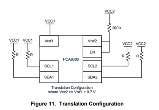
Need your expertise on this. Our customer is currently using the PCA9306 as a level shifter configured in switch configuration (Figure 10 of datasheet).

Operating conditions are as follows:
VREF1 = 1.8V
VREF2 = 3.3V
EN pin is tied to MCU which has a high logic level of 3.3V

Should they be using the translation configuration instead, or can this configuration still work?

Are there any potential risks? Asking for your help as they've already made a significant number of PCBs using this configuration.


Kind Regards,

Jejomar

  • In the switch configuration, the two reference voltages are identical. That configuration is not the switch configuration.

    If the EN pin is tied directly to 3.3 V, then the switch allows all voltages between 0 V and about 2.5 V to pass through unchanged. This means that a current from the 3.3 V supply can leak into the 1.8 V supply.

    In the translation configuration, the EN pin should be driven from an open-drain output. Can you change the MCU output? (In the worst case, it should be possible to configure the MCU pin as a high-impedance input.)

  • Hi Jejomar,

    As Clemens said since your VREF voltages are not identical you have to use the translation configuration:

    I agree with what Clemens says, the biggest concern is that current can leak from the 3.3V supply into the 1.8V supply. Are you able to modify the PCB so that the device is in the translation configuration?

    Best,

    Chris

  • Hi Clemens and Chris,

    Many thanks for your helpful inputs. We will certainly look into proposing the PCB changes and to use the translation configuration instead.

    Just a final clarification about our customer's current configuration - what if the enable pin is connected to the 3.3V through the MCU internal pull up resistor? In this configuration the Vref2 and enable will be connected to the 3.3V through a pull up resistor. But it will still violate the data sheet because vref2 and enable are not shorted together? Would this still allow the current from the 3.3V supply to leak into the 1.8V supply?


    Kind Regards,

    Jejomar

  • In the translation configuration, EN and VREF2 must be shorted together in order to pull down EN to the appropriate voltage. Otherwise, the EN voltage is too high, and all pins on the VREF1 side (including VREF1) are not clamped below 2.5 V.

  • Hi Jejomar,

    To add onto what Clemens said, if EN is sitting at VCC2 the gate voltage would be equal to VCC2. Any voltages above VCC2-Vth would then form a voltage divide between side 1 and 2. Side 1 would then site above VCC1 and side 2 would sink below VCC2. The device would no longer function as expected.

    Best,

    Chris