
- Ask a related questionWhat is a related question?A related question is a question created from another question. When the related question is created, it will be automatically linked to the original question.

Hi,
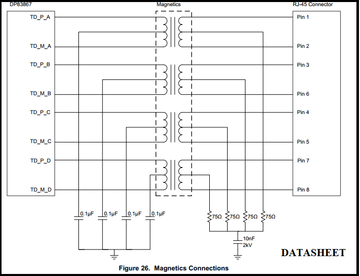
Based on the description available on page 92 of the DP83867CS datasheet (SNLS504B) the pin mapping between magnetics and RJ45 is given (Image attached)
Channel A to Pin 1,2
Channel B to Pin 3,6
Channel C to Pin 4,5
Channel D to Pin 7,8
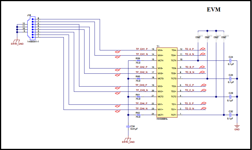
But on the schematics of DP83867E SGMII EVM (SNLU209 ) available on page 12 the connections are shown as below (Image attached)
Channel A to Pin 7,8
Channel B to Pin 4,5
Channel C to Pin 3,6
Channel D to Pin 1,2
I am using DP83867CS PHY to implement SGMII with MAC available inside Kintex-7 FPGA.
Which Pin mapping have to be followed in the PCB design under progress?
How the MDI signals behave in SGMII? Do the Channel A&B are transmit lines and Channel C&D are receive line? What is their operating Frequency in SGMII mode?
Thanks and Regards
DEEPAK V


