This thread has been locked.

If you have a related question, please click the "Ask a related question" button in the top right corner. The newly created question will be automatically linked to this question.

DS90CF386: Mapping to iMX6

Genius 5355 points
Other Parts Discussed in Thread: DS90CF386

Hi Support,

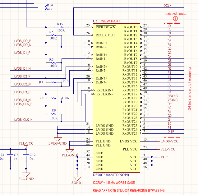
Going to use the DS90CF386 to convert LVDS signal from Freescale iMX6 dual light to RGB display.

Currently I have a question about the RGB signal mapping from the TI part to the display connectors (using JEIDA mapping).

Please help to check the signal if we have done correctly.

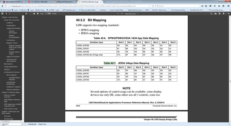
Attached the schematic for the TI de-serializer and the bit mapping of the LVDS signals from imx6 dual light.

Thanks.

  • Hi Shaun,

    I reviewed your schematic, and I think there are some issues with the mapping. It looks like in the schematic that RxOUT0-27 just goes sequentially from LVDS_DATA0 to LVDS_DATA3. In reality, the deserializer does not output RxOUT0-27 sequentially from the LVDS outputs. The deserializer outputs are actually mapped as follows in the datasheet:

    This diagram was originally taken from the DS90C385 serializer to show how the LVCMOS inputs are mapped onto the LVDS pairs, but this mapping also applies to how the serialized LVDS is mapped out of the DS90CF386.

    Therefore, if you reference the DS90CF386 output bit-mapping, your mapping for RGB bits in the JEIDA format should be as follows:

    Output RGB Bit
    RxOUT0 R2
    RxOUT1 R3
    RxOUT2 R4
    RxOUT3 R5
    RxOUT4 R6
    RxOUT5 R1
    RxOUT6 R7
    RxOUT7 G2
    RxOUT8 G3
    RxOUT9 G4
    RxOUT10 G0
    RxOUT11 G1
    RxOUT12 G5
    RxOUT13 G6
    RxOUT14 G7
    RxOUT15 B2
    RxOUT16 B0
    RxOUT17 B1
    RxOUT18 B3
    RxOUT19 B4
    RxOUT20 B5
    RxOUT21 B6
    RxOUT22 B7
    RxOUT23 CTL
    RxOUT24 HS
    RxOUT25 VS
    RxOUT26 DE
    RxOUT27 R0

    Thanks,

    Michael

  • Hello, I am working on a nearly identical application interfacing the iMX6 to the DS90CF386 but I am confused by this answer.  In the IMX6 LVDS mapping they encode the R-G-B data into the 7 "slots" for the Data0 to Data3 channels.  Are you saying that the Data_0 Slot 1 is output onto RxOUT6 and Data_3 Slot 5 is output to RxOUT_5?

    Thanks in advance

    Patrick

  • Hi Patrick,

    Yes, that is correct. You must match up the RGB bit in the JEIDA slots with the corresponding RxOUT (or in the diagram, TxIN) bit that occupies the same slot position shown in Figure 10.

    I agree with you that this is confusing, but this is an implementation that has long been in place by TI and other LVDS SerDes vendors. For more information, please see Application Note SNOA014. The mapping should match up with the listing in Table 1 of the app note.

    Thanks,

    Michael