This thread has been locked.
If you have a related question, please click the "Ask a related question" button in the top right corner. The newly created question will be automatically linked to this question.
Hello,
I connected the SN65HVD102 with my MCU.
And the MCU has a UART-bootloader with same RX and TX lines from SN65HVD102.
Now i want to connect these TX, RX lines with a FT232RL von FTDI and use the bootloader
to program the MCU. But I am not able to communicate with the MCU. Remove the SN65HVD102
then i can communicate with the MCU again. Are there possibility to do this while
the SN65HVD102 is connected?
Hi Michael,
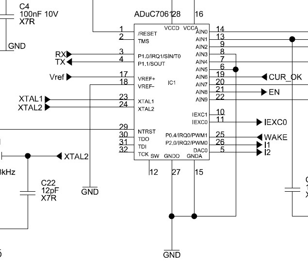
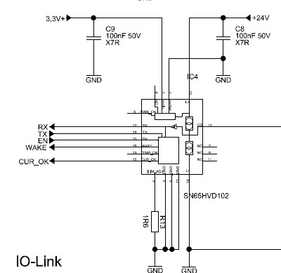
here are the schematics. I have 2 Pull-up resistor for RX, CUR_OK with 10kOhm and 1 Pull-down 10kOhm for EN Pin.
The board will be connected to external FTDI-USB-RS232 Board.
RX ---> TX_FTDI
TX ---> RX_FTDI and GND.
The IO-Link Device is not enable. First i want to program the ADUC7061.
Like i said before when i removed the RX, and TX lines of SN65HVD102 and connected directly the SIN(RX) and SOUT(TX) of the ADUC7061 to
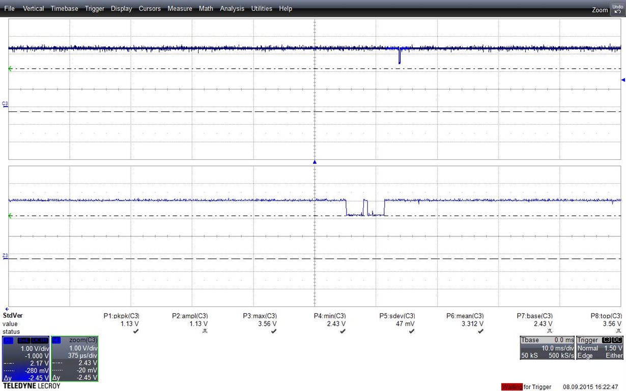
USB-RS232 Board then i can program the ADUC7061. When I connected them all together then i can not program the ADUC7061. Under Scope i saw
that the logic Signal on RX line can not be down to low level.
Best Regards
Ngoc
Van,
Considering that the logic signal on the Rx line is not reaching a low level, it is possible that the line is being pulled high by the Rx output of the SN65HVD102. One point to consider is that the Rx line is not affected by the EN pin, meaning that the RX pin will not be in a high impedance state under any EN pin condition. A possible solution may be to add a small resistor between the SN65HVD102 Rx line and the microcontroller Rx input.
Best Regards,
Casey McCrea
Hello Casey,
Thank you for your answer. I tried a 100Ohm resistor between the SN65HVD102 Rx line and the ADUC7061 Rx but it did not work. Now i have another problem with the wake up line. The SN65HVD102 did not generate wake up signal. I measured the signal on C/Q and Rx Lines. It seems to be correct. The wake up pulse is 83us width. The wake up signal stays high. Do I need to connect another Output pin PWR_OK, TEMP_OK with pull up resistors?
Best Regards,
Ngoc
Van,
If the 100 Ohm resistor between the Rx lines did not work, your design may need a more complicated solution. Based on your second post, it seems like the Rx line is exhibiting switching behavior but is not reaching a low logic level. Is that correct? Do you have any scope pictures of the Rx line?
As for the new problem with wake up, you should connect the PWR_OK and TEMP_OK pins with pull up resistors as per this example diagram in the data sheet:
The wake up pulse time you are measuring seems correct, but after the PWR_OK and CUR_OK lines are connected with pull up resistors, try probing these lines during operation to diagnose any problems. A low level at the PWR_OK pin could indicate either Vcc is too low or VL+ is too low. A low level at the CUR_OK pin indicates that CQ current is at the internal limit for longer than the maximum allowed time. You can refer to this diagram:
You could also probe the TEMP_OK pin to see if the device is overheating.
Also, since you mentioned in your first post that you are attempting to program the MCU with the bootloader during this process is it possible that the EN signal going to the HVD101 is not correct? This would be another pin to probe during testing to make sure the device is enabled.
Finally, what size resistor are you using for the current limiting?
The Problem with the rx line is also resolved. The Solution is like you said, a Serial resistor between Rx-Line MCU and HVD102, with a 330Ohm Resistor not 100Ohm like my post before and it works.
Thank you so much for your helps and your efforts.
Best regards,
Ngoc