Other Parts Discussed in Thread: PSPICE-FOR-TI, ADC128D818
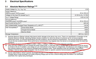
The ISO7763 has esd protection diodes, but a Vmax and Vmin is specified as well as a current max IN in the input and output pins. The max output current is 2mA and the max input current is 2µA.
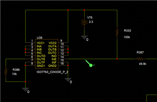
We have a resistive divider network attenuating the input signal (highest I/P) to ±10 V without ISO7763. Connect the ISO 7763 and the input is limited to 3 or 4 V and input pin current is higher than 2µA. the corresponding output pin voltage is good. We are exceeding the Max Vin and input current on the pin, but the part simulates fine. It would appear that the spice model assumes the device is operating in the proper range.
I need to add the diode BV which is 6V. Vfb appears to be 0.5. I need to include the max diode current 2µA too. The ISO7763 model appears to run on the correct IDEAL conditions. How do I incorporate these parameters into the model to show real word results? I assume I would add them in the INPUT subcircuit in the ISO7763 .lib file.
I called the tech support line. I was told to submit a ticket. I submitted a ticket, and now I am told to submit another ticket to a different group. I really need an answer how to do this.
Sincerely,
Joe