This thread has been locked.

If you have a related question, please click the "Ask a related question" button in the top right corner. The newly created question will be automatically linked to this question.

ISO6761: 750VDC for 10sec seems to damage '6761

Part Number: ISO6761
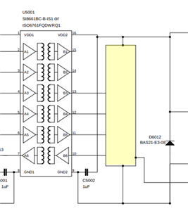
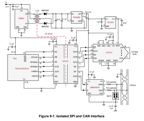
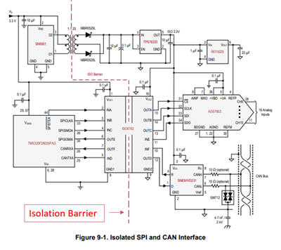
Other Parts Discussed in Thread: SN6501, ISO6762

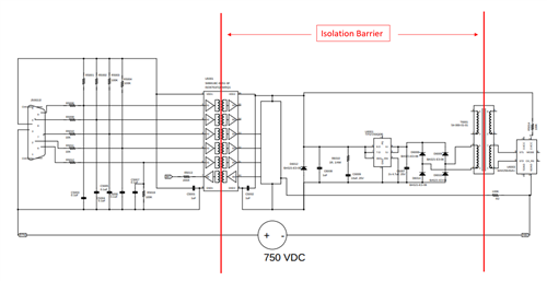
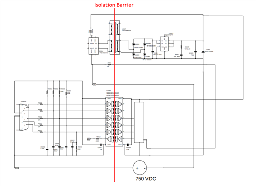
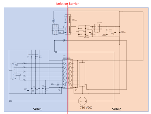
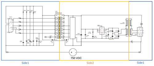
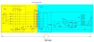
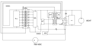
I check the isolation of my complete board by applying 750VDC across the isolated regions.

Often I'm finding the IS6761 being damaged after this test.  

This doesn't always happen (the damage) but I have no other clue as to why the ISO6761 is found to be failing.

Ramping up to 750VDC over 10sec, dwell 10sec, ramp down to 0V over 10sec.

What might be happening here?

  • Hello Paul,

    Thank you for reaching out. ISO6761 can provide Maximum working isolation voltage (Viowm) of 2121 VDC across the isolation barrier (from GND1 to GND2), therefore 750 VDC across the isolation barrier should not be an issue.

    Can you please provide more information on your application (see below questions)? Can a schematic or diagram of the test be provided?

    1. How/Where is the 750 VDC applied? Applying 750 VDC from GND1 and GND2 should not be an issue, however, if applying the voltage across I/O or supply pins can cause device damage.
    2. What is the failure mode that you are seeing (how are the devices damages and how frequently)?

    Best,
    Andrew

  • Hello Paul,

    I hope all is well. Can you please provide responses to the above question? If the issue was solved or found not to be the ISO6761, please let us know so we can close this post.

    Best,
    Andrew 

  • Andrew,


    The attached diagram shows how the 750V is applied.

    The part fails with symptoms of output not switching with input and part body getting warm to hot.


    Thank you for your quick response.HiPot.pdf

  • Hi Paul,

    Thanks for providing the diagram. I have a few follow up questions regarding your setup. Could you explain how the negative terminal of the voltage is connected to the ISO6761? Additionally, what is the rectangle in the diagram on side 2 of the device representing? I've highlighted the portion below I'm referring to for your convenience

    Could you also explain how the device is damaged? Are you seeing physical damage on the device or is the output a constant or unexpected low/high after testing occurs? Are there any shorts from ground to VCC or ground to an I/O pin?

    Regards,

    Darrah

  • The part fails with symptoms of output not switching with input and part body getting warm to hot.  No other circuitry is damaged.

    The negative of the 750V is connected as shown.  Indirectly connects to the VDD terminal of the ISO6761.  The  rectangle is all other circuitry of the design including a microprocessor.  The I/O of the ISO' go to this micro.

  • Can you measure the resistance of each pin to their respective ground? Can you also measure the resistance between GND1 and GND2 pins?

    Where is the MAX256 VCC pin connected to? Is it connected to VDD1 of the ISO6761?

  • The in circuit resistance from any ISO6761 pin to its ground can be zero because they are driven by low impedance sources.  GND1 to GND2 is >100MOhm.  Exactly what are you looking for with these measurements?

    The MAX256 VCC is not directly connected to VDD1.  There is a switching supply and EMI filter in between.

    What do these parameters have to do with your ISO6761 isolation?  Doesn't it isolate these regions with better than 750VDC withstand?

    Maybe we can focus the conversation on what situations could cause the IC to fail.  Then I can verify if my circuit is doing that and then fix it.  I'm not even sure that the hipot test is the culprit yet.  The IC may be failing from some other misapplication.  I'd like to be able to say that the hipot is not the source of my problem, at least.

  • Hello Paul,

    The MAX256 VCC is not directly connected to VDD1.  There is a switching supply and EMI filter in between.

    From what you've mentioned it looks like MAX256 VCC and ISO6761 VDD1 share the same ground (GND1 of ISO6761 and GND of MAX256 are the same). If this is true, then the 750V DC is not being applied across the isolation barrier of ISO6761. Therefore, the isolation barrier of the ISO6761 is not being stressed and it does not look like there is any damage to the isolation barrier.

    Since 750V is being applied on the GND1 side where the I/O pins can only handle up to 6V max, it is possible that the device I/Os are physically damaged. Therefore, we would like to confirm if this is the case, and it would help if you can provide the resistance values between the pins and their respective grounds to determine if the device is physically damaged. Can you measure the resistance at the pins with the device de-soldered from your PCB? This way the measured resistance will be representative of the isolator itself and not the system it is built into.

    Sorry for asking so many questions, the reason we are asking so many questions is because it looks like the 750V you are applying is being applied on side1 of the ISO6761 only and not across the isolation barrier of the ISO6761. The I/O pins on side1 are low voltage pins and will not withstand anything more than 6V and we believe during this test the I/O pins are damaged. To confirm this please share the requested information. If anything is not clear, please let us know.

    Regards,

    Darrah

  • Refer to the block diagram. 

    750V(-) is indirectly tied to ISO6761 VDD2(pin16)/GND2(pin 9) and all of the other circuitry on the right side of the diagram, including the MAX256.  

    750V(+) is tied directly to ISO6761 GND1 (pin 8)

    I did not know you wanted me to look at the damaged device.  I'll see if the I/O's are damaged by removing the bad IC from the circuit.

    I have no complaint about questions.  Knowing why I'm doing a circuit measurement helps me get the correct data.

    What if we discover that one of the ISO' pins is shorted?

    The only connections in the circuit are to the 750V.  How could this connection to 750V damage one of the ISO' inputs?  What situation would allow this to happen?

  • Hi Paul,

    Digital isolators like the ISO6761 have two circuits that are isolated from each other and each circuit requires its own power supply, which is isolated from the other one. One way to achieve this is to power one side of the isolator using an available power supply and the other power supply is generated using  an isolated power solution like the SN6501 or MAX256. The isolated power supply then creates an isolated power supply for the other side. This way both sides of the device have a power supply, but the two supplies are isolated. Please see the schematic below, which shows this kind of application.

    The dashed red line in the schematic represents the isolation barrier. Everything to the left of the isolation barrier is side1, and everything to the right of the isolation barrier is side2. Since the two sides are isolated, each side has its own respective power supply and ground. As you can see the transformer driver (SN6501) uses the same ground as GND1 of the digital isolator (ISO6762) and is on the left side of the isolation barrier.

    Based on your schematic and what you've described it appears that your application is similar. The MAX256 in your schematic is drawn on the right side of the ISO6761, but electrically the connections would place the MAX256 on the left side of the isolation barrier, which means the MAX256 GND would be the same as the ISO6761 GND1. One other reason we think that the MAX256 is on the left side because the isolated power generated from the MAX256 is connected to the ISO6761 VDD2 (right side), which means that the MAX256 VCC would come from the left side of the ISO6761.

    Can you confirm if this is how your application is designed?
    I want to make sure that I am understanding your design correctly so I can provide accurate feedback.

    Regards,
    Darrah

  • Darrah,

    Yes, that is the same scheme that I have for separating the two isolated circuits.

    From this discussion so far, I'm thinking my ISO' failure is not from the hipot test.

    Could a floating input pin on the ISO6761 cause it to be damaged when powered up?  My isolator may have had this situation.

  • Hi Paul,

    Thanks for confirming your application. A floating input pin would not cause any damage to the ISO6761, unused channels can be left as no connect.

    I believe the damage is due to how the 750V is being applied to the ISO6761. The 750V appears to be applied across side1 of the ISO6761 instead of across the isolation barrier (side1 and side2). Applying a voltage >6V to one side of the ISO6761 would result in damage on the side seeing the high voltage.

    As we discussed in the previous posts, the MAX256 is on the left side of the isolation barrier (side1), therefore the MAX256 will share a ground with ISO6761 GND1. This means the MAX256 GND and ISO6761 GND1 are the same ground. In the schematic you provided, the 750(+) is connected to the ISO6761 GND1, and the 750V(-) is connected to a node that includes the MAX256 GND. But since the ISO6761 GND1 and MAX256 GND are shared this means the 750V(+) and 750(-) are connected to the same ground. So the 750V, with respect to the isolator, is being applied to only the ISO6761 GND1 pin, or side1 of the ISO6761.

    If you find that the I/O pins are shorted this would confirm that the voltage is being applied to only side1. In order to apply the 750V across the isolation barrier (side1 and side2), the 750(-) would need to be connected to the ISO6761 GND2 pin.


    Regards,
    Darrah

  • Darrah,

    I don't think you're looking at the correct diagram.  I've attached it again for your reference.

    750V(-) is attached to the MAX256 circuitry which is on the GND2 side of the ISO6761 (GND2 is pin 9).

    750V(+) is attached directly to GND1 side of the ISO6761 (GND1 is pin 8).

    You can see then that the 750V is applied across the ISO6761 isolation barrier.

    The MAX 256 is at the rightmost of the diagram not attached anywhere near GND1 at the left side of the diagram.

    Maybe you could highlight the diagram to show the paths of how you think the 750V appears at the ISO6761.

    1665.HiPot.pdf

  • Hello Paul,

    One way to achieve this is to power one side of the isolator using an available power supply and the other power supply is generated using  an isolated power solution like the SN6501 or MAX256. The isolated power supply then creates an isolated power supply for the other side
    The MAX256 in your schematic is drawn on the right side of the ISO6761, but electrically the connections would place the MAX256 on the left side of the isolation barrier, which means the MAX256 GND would be the same as the ISO6761 GND1.
    Yes, that is the same scheme that I have for separating the two isolated circuits.

    In your last post you confirmed that your application uses the MAX256 on side1 to generate an isolated power supply for side2. Is this not actually the intent of your design? If the MAX256 is not generating an isolated power supply, what is its function?


    The confusion between side1, side2, GND1, and GND2 is coming from the way the schematic is organized. Normally when making a schematic for an isolated system all components are placed with respect to the isolation barrier. The isolation barrier is only represented once to make a clear distinction between the two sides. You can see this in the reference design below. Everything to the left of the dashed red line is side1 and everything to the right of the dashed red line is side2.

    However, in your schematic you can see the isolation barrier is marked in two places, on the ISO6761 and the MAX256.

    If your schematic is redrawn with the isolation barrier represented once, your application would look similar to the image below. Please note how the updated schematic is similar to the example digital isolator with an isolated power source reference design I shared previously.

    With all the components placed with respect to the isolation barrier, there is a clear distinction between side1 (blue) and side2 (orange), which are marked in the image below.

    As mentioned in the previous posts, since the two sides are isolated, each side has its own respective power supply and ground. This means the components on side1 (blue) must share the same ground, and all the components on side2 (orange) must use a different ground. For your application, this means the MAX256 and the ISO6761 share the same ground because they are both on side1.

    Now using this logic on the original schematic, the different sides of the isolation barrier would look like the image below.

    You can see that both the 750V(+) and the 750V(-) terminals are connected to side1. Even though the MAX256 circuitry is physically placed on the right side of the schematic, it is still connected to the left side of the digital isolator.

    Please let me know if anything is not clear. 

    Regards,

    Darrah

  • Darrah,

    Your interpretation of my block diagram are not correct.

    My terminology is probably not matching yours.

    I've attached the block diagram again but now highlighting the two isolated regions in yellow and blue.

    The MAX256, transformer, and all other circuitry on the right side of the diagram belong to isolation region named GND2.

    GND1 isolation region is in yellow.

    6518.HiPot.pdf

  • Hello Paul,

    In an isolated system, there are two circuits, each sitting on its own ground reference point, which are isolated from each other. All components in the system have to refer to one of these two grounds

    Can you please confirm if the MAX256 GND pin is connected to GND1 or GND2 of the ISO6761? 

    Regards,
    Darrah

  • Darrah,

    The MAX256 has its own GND reference that is neither GND1 nor GND2.  This GND is very near the level of GND2 however.  The MAX256 does not directly power the ISO6761 but is used to generate the GND2 power supplies.  That is why I lump it in with the GND2 circuitry.  It has nothing to do with the GND1 circuitry and is totally isolated from it.  Please refer to my block diagram to see where GND1 and GND2 are.

    My circuit is not the same as your circuit of course.

  • Hello Paul,

    Thanks for explaining more about your setup. Based on your description, it sounds like there is 2 levels of isolation with 3 isolated supplies.

    • Supply1 is referenced to GND1 and is powering VDD1 of the ISO6761.
    • Supply2 is referenced to GND2 and is powering VDD2 of the ISO6761 and all the other components in the rectangle of the schematic like the MCU.
    • Supply3 is reference to the MAX256 GND and is powering MAX256 VCC.
    • All 3 supplies are isolated from each other.

    We understand the need for isolation with the ISO6761 and why isolation is necessary between VDD1 and VDD2 but do not understand why there is isolation between the MAX256 VCC and ISO6761 VDD2. The MAX256 is powered by a supply of either 3.3V or 5V and the ISO6761 VDD2 requires a similar voltage, why not power VDD2 directly? Why is the isolated supply necessary?

    Were you able to measure the resistance of all the I/O pins with respect to their local ground and the resistance between pins GND1 and GND2 of the ISO6761? As mentioned in the earlier posts, providing these values will help determine if the failure is between the outputs and GND or between GND1 and GND2. Please measure these values on a bad/damaged unit that has been de-soldered from the PCB.

    If  you could share a complete schematic that would help clarify a lot about your design and answer more questions. The more that we know about your application and testing the quicker we can solve the problem you are facing.


    Regards,
    Darrah

  • I may not share the complete schematic with you.

    I've redrawn the block diagram to show exclusively the power supply connections.

    VEXT is not in the circuit during hipot test.

    750VDC is applied during hipot test.

    All circuitry not in GND1 (dashed outline) is referenced to GND2 in some way.

     HiPotPwrSupply.pdf

  • Hi Paul,

    Thank you for this redrawn schematic. Including the additional transformer coil connections makes it much more clear how the MAX256 is being used to power your application. It is now clear that the 750V is being applied across the isolation barrier. We would not expect 750V to cause any damage to the isolation barrier. However, the damage you are seeing could be linked to another aspect other than the barrier. In order to determine if the barrier itself is being damaged or if I/Os on the ISO6761 are being damaged could you provide the resistance measurements of both the I/Os pins to their respective GND and resistance measurement of GND1 to GND2? 

    If you are okay with sharing your complete schematic over email instead of this forum, we can reach out over email instead.

    Regards,
    Darrah

  • Darrah,

    I think we've gone far enough with the investigation for now and this issue can be closed.

    You've confirmed that the application of 750VDC, as drawn, would not in any way cause the ISO6761 to fail.

    Finding other conditions where the inputs could be getting overvoltage can be left to me.

    -Paul

  • Hi Paul,

    I will go ahead and mark this thread as closed. If you have any additional questions in the future, feel free to make another post.

    Regards,
    Darrah